When it comes to powering tiny devices for a long time, coin cell batteries are the battery of choice for things like keyfobs, watches, and even some IoT devices. They’re inexpensive and compact and a great choice for very small electricity needs. Their major downside is that they have a relatively high internal resistance, meaning they can’t supply a lot of current for very long without decreasing the lifespan of the battery. This new integrated circuit uses a special DC-DC converter to get over that hurdle and extend the life of a coin cell significantly.
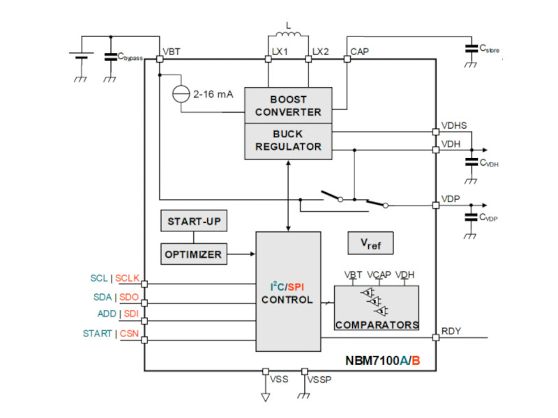
A typical DC-DC converter uses a rapidly switching transistor to regulate the energy flow through an inductor and capacitor, effectively stepping up or stepping down the voltage. Rather than relying on a single converter, this circuit uses a two-stage system. The first is a boost converter to step the voltage from the coin cell up to as much as 11 volts to charge a storage capacitor. The second is a buck converter which steps that voltage down when there is a high current demand. This causes less overall voltage drop on the battery meaning less stress for it and a longer operating life in the device.
There are a few other features of this circuit as well, including an optimizer which watches the behavior of the circuit and learns about the power demands being placed on it. That way, the storage capacitor is only charged up to its maximum capacity if the optimizer determines that much charge is needed. With all of these features a coin cell could last around seven times as long as one using more traditional circuitry. If you really need to get every last bit of energy from a battery, though, you can always use a joule thief.


I smell B.S., energizer all over again.
It does seem like a drastic solution to a simple problem. All that should be necessary is a big capacitor across the coin cell.
Depending on what you are powering, you may need a regulator to convert the battery voltage into the load voltage; but it would be a lot simpler than this design.
PS: a SEPIC (Single Ended, Primary Input Converter) is often used when the input voltage can be higher or lower than the output voltage.
First things first – as a 3x4mm-ish QFN16, this isn’t exactly friendly to the average maker / hobbyist, but it’s cool if you’re equipped to handle tiny SMD packages.
Your big cap + battery is one solution, but would result in significant current draw from the battery to recharge the capacitor. Yes, simple options like a current limiting resistor exist, but this is wasteful in a micropower system.
Small batteries have significantly reduced [milliamp-hour] capacity with higher current draw. This is especially notable with some chemistries (like Thionyl Chloride Lithium cells), which have extremely high capacities at low currents (sometimes as low as several mA) but cannot handle larger currents.
I’m not sure how much simpler you can get than a single-chip design that uses only a handful of components. It takes up very little board real-estate, and most of all, is already engineered and well-characterized, which shortens the development time of a product in which it is used; Nexperia has done the engineering work for you. (I’m not promoting the product, just pointing out why packaged systems like this can be a good idea). I’m imagining they would also provide some kind of engineering support to firms who are designing a high-volume product that will use these.
That said, as a professional engineered, commodity product, it’s absolutely the opposite of a hack, so I’m not quite sure how it fits on HaD, but it’s interesting nonetheless.
Crikey, I think I spotted a Dave Jones in the wild, he’s in his natural element debunking bs electrowizard claims.
All of you are not understanding the main issue and the solution proposed.
The main issue is that the coin cell effective capacity decreases a lot if the load current is high. Even spikes can strongly reduce the capacity, despite if the average current is low.
A typical IoT device sleeps most of its time, and when it wakes up, it draws some (e.g. 10-20 mA) peak current for the radio, for a short time. This peak might seem low, but on a small battery such SR66 is huge, and can reduce a lot the battery life, despite the average current might be in the microamperes range.
Using a boost, you can very slowly ( i.e. with a very tiny peak current) charge a reservoir capacitor, which can be discharged later when needed (during TX), by the buck, providing a regulated voltage to the MCU with the current peak it needs. Because of the relatively high voltage at which the reservoir capacitor is charged (with respect to the buck output voltage) you can store use the majority of the energy stored in the capacitor, because you can discharge it almost completely (down to the buck output voltage).
Instead -you might do the math- placing a capacitor in parallel to the battery requires a huge capacitance, even to reduce by a little bit the battery current for modest spikes.
Finally, a large capacitor in parallel to the battery is detrimental because when the battery is inserted, a huge current spike occur, damaging it (we made some project and we found this was the issue on shorter than expected coin battery life. By reducing the input cap, the device showed the expected lifetime).
Now I want a few samples in the form of a small board with a battery holder on one side and a “dummy” battery shell on the other, to snap into existing devices and see how it behaves in real-world conditions…
yeah, this would need to integrate into hardware typically used for the micro-IoT devices that run on coin cells. these applications aren’t exactly looking for another IC to find room for.
I’ve wondered for a while, step up then step down.. is this how power supplies work when the output voltage is very close to the input voltage?
For example, I have a device which runs of 12V, requires clean power and has a car cigarette-plug adapter. It works both when the car is turned on and so above 12V but also when it is off and at 12V.
I think the typical topology for this application is a buck-boost converter: https://en.m.wikipedia.org/wiki/Buck%E2%80%93boost_converter, or a Ćuk converter when less ripple is required. The former uses only a single capacitor, diode, and inductor just like a buck or boost converter, while the latter has two each of the inductor and capacitor. All of these designs have a single switch.
These differ from the design in the article, which has separate step-up and step-down stages each with their own switch; it’s this that allows the design to keep the battery discharge current low while providing more power from the capacitor when it’s needed.
While a buck-boost (or other up/down DCDC converter) is the device that typically comes to mind for something like this, the reality is that buck converters or even LDOs are much more common for such an application.
95% of the time it’s more like: 12VDC nominal supply from a car battery? Use a buck converter (or an LDO if you don’t care about heat, efficiency and possibly device lifetime) that’ll take an input as high as 18V or 24V and step down to 5V for your circuit.
The buck-boost or similarly expensive topologies are only needed when your required downstream circuit voltage is actually close to the nominal 12V voltage of your supply.
The device is not a buck-boost topology as it might seem. So no Cuk, Sepic or similar topology.
It is operating in boost mode to charge the capacitor up to eg. 11V and then when the application demands high current it operates in buck mode to consume the energy stored in the capacitor and deliver it to the consumer with a fixed voltage.
Uh yeah, we weren’t talking about the article. That was a reply to Twisty Plastic’s more general question about power supplies.
It seems like a strange concept, adding additional current draw, to somehow extend the life of a battery.
I can perhaps envision something that possibly draws a lot of current for a short amount of time needing some sort of smoothing capacitor to mitigate damage, but surely something that is trying to run for a long time on a coin cell isn’t going to be trying to dead short the terminals.
[ Unless it’s some time delayed device that want’s the coin cell to get very warm. Then you probably only expect it to do that once anyway. :D ]
It is a brilliant idea for some seldom usecase. For example a device that most of the time use a few microamps, perhaps to measure something and once a day it switch on an ESP8266 so send the data to WLAN. Than it needs 100mA for 1-2s. A single capacitor for this is bad and huge.
The next level of brilliance would a device with an input that can work with the floating voltage of a solar cell. :)
Olaf
There is some point to this chipset as it is applying a concept called peak shaving.
E.g. instead of drawing a 200mA current peak for X s, it will draw 20mA for 10X s, or 8mA for 25X s.
Since losses in ESR of the battery scales with P=I^2*R, it could in theory reduce those losses by a factor of 100 in those applications.
But the question is whether it matters. First, you won’t run a 200mA load on a normal coin cell as with e.g. 10Ohm internal resistance its basically a short and so it wont work (there goes you apples to apples comparison). Then take say 50mA, it may have say 0.5V voltage drop @ 10Ohm ESR, so 2-2.5V going into the load. That means that still only 20-25% is losses from ESR. In theory you could reduce that to single-digit percentages. Well great, but thats not really the multifold increase they are talking about.
And that is not including the quiescent current draw, which is far from zero, as the DC/DC is “only” 50% efficient at 1mA(if I read the charts correctly?). Plus it cuts out at 2.4V, which is decent, but doesn’t make it great for e.g. AAA applications (although you probably also want a bit more output current for that).
I really do wonder how the comparison looks like if you were to just put a mF supercap in parallel to the coincell..(not too big as it will increase leakage) Large capacitances to soak up current spikes is a large recommendation anyway.
Looking at the datasheet all the caps in the example circuit are MLCC plus the inductor will be tiny as well – supercaps can be pretty bulky so this may well be the reason to do this – it provides similar functionality to large capacitor but with less space – or if not with less space overall, than at least thinner, which can be important for some applications.
> I really do wonder how the comparison looks like if you were to just put a mF
> supercap in parallel to the coincell.
It is possible that this will destroy your coincell because it is a shortage on
the coincell for a very long time until it charge your big supercap.
Olaf
Why does nobody read the linked article? Figure 4 answers the question with the capacitor in parallel to the cell.
Good thing is that the dcdc does not run continously and standby current is extremly low. What is not mentioned in the article: cr2032 will reduce drastically its capacitance when high current pulses are drawn. That the voltage drops due to internal resistance is only one aspect to it.
Cr2033 is known as beeing a “bad battery” despite the good energy density due to those 2 effects.