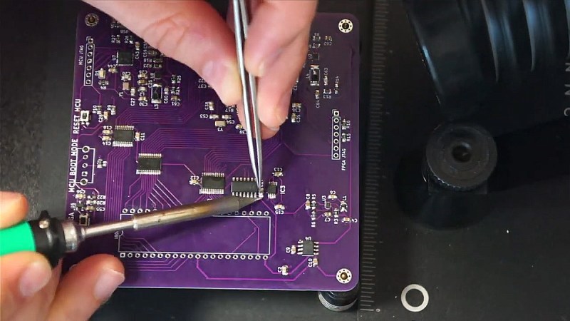
If you’re into retro CPUs and don’t shy away from wiring old-school voltages, [Mark]’s latest Intel 8080 build will surely spark your enthusiasm. [Mark] has built a full system board for the venerable 8080A-1, pushing it to run at a slick 3.125 MHz. Remarkable is that he’s done so using a modern Microchip FPGA, without vendor lock-in or proprietary flashing tools. Every step is open source.
Getting this vintage setup to work required more than logical tinkering. Mark’s board supplies the ±5 V and +12 V rails the 8080 demands, plus clock and memory interfacing via the M2GL005-TQG144I FPGA. The design is lean: two-layer PCB, basic level-shifters, and a CM32 micro as USB-to-UART fallback. Not everything went smoothly: incorrect footprints, misrouted gate drivers, thermal runaway in the clock section; but he managed to tackle it.
What sets this project apart is the resurrection of a nearly 50-year-old CPU. It’s also, how thoroughly thought-out the modern bridge is—from bitstream loading via OpenOCD to clever debugging of crystal oscillator drift using a scope. [Mark]’s love of the architecture and attention to low-level detail makes this more than a show-off build.


When I first read the summary, I thought the 8080 itself was implemented within the FPGA.
I didn’t realize that the FPGA was just a support system for an actual 8080.
That’s what I thought as well. The internal 8080 blocks should be easily implemented. Yes, program memory would be external.
If I recall correctly, these early members of the x86 (8080, 8085?) family needed a lot of supporting logic in order to constitute a working general purpose computer. Probably a little easier to find a working Intel 8080 CPU these days than it is to source the Intel 8224, Intel 8228, and other presumably less common parts.
Fun project! It would be cool to slightly extend it with 2 rows of 40 pin headers (one connected to voltage convertors, other to DIP40 socket) to make it a generic 40-pin legacy CPU “adapter”.
can run doom 1993?