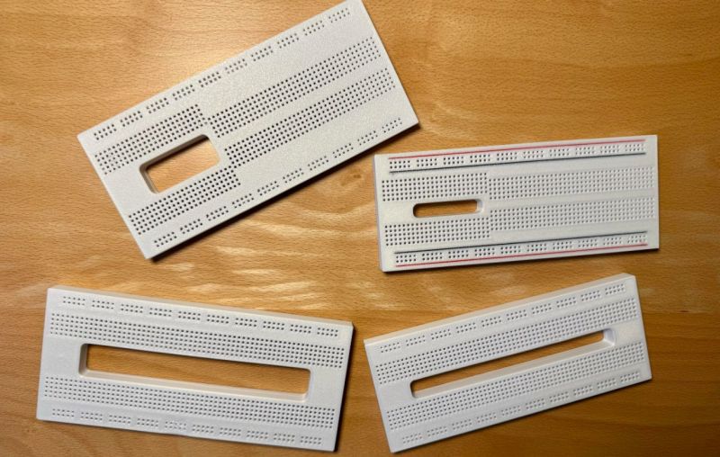
Although off-the-shelf breadboards are plentiful and cheap, they almost always seem to use the same basic design. Although you can clumsily reassemble most of them by removing the voltage rail section and merging a few boards together, wouldn’t it be nice if you had a breadboard that you could stick e.g. one of those wide ESP32 development boards onto and still have plenty of holes to poke wires and component leads into? Cue [Ludwin]’s 3D printable breadboard design that adds a big hole where otherwise wasted contact holes would be.
The related Instructables article provides a visual overview of the rationale and the assembly process. Obviously only the plastic shell of the breadboard is printed, after which the standard metal contacts are inserted. These contacts can be ‘borrowed’ from commercial boards, or you can buy the contacts separately.
For the design files there is a GitHub repository, with breadboard designs that target the ESP32, Raspberry Pi Pico, and the Arduino Nano. An overview of the currently available board designs is found on the Hackaday.io project page, with the top image showing many of them. In addition to the single big space design there are also a few variations that seek to accommodate just about any component and usage, making it rather versatile.


how about using the “wasted space” as an additional voltage rail on the full length holes?
Why is nobody selling half-breadboards? Or sawing existing breadboards in half?
I’ve always sawed them in half, stuck an dev board into them, and peeled the adhesive & stuck them onto a bit of plastic or plywood. Takes a minute or two. Less if you have a bandsaw.
There are breadboards on ali where you can detach each power rail, so I do this:
Buy 2 breadboards, detach only 1 power rail per board, mount the MCU devkit in the free space of board A and B where the power rails were stripped.
It’s flimsy but works universally for any size of a board, and it is the only solution for a 3D-printerless serf like myself.
This helps you visualize it:
[https://i.imgur.com/cBfM7VN.jpeg]
Or as the article says:
Although you can clumsily reassemble most of them by removing the voltage rail section and merging a few boards together
I mean it’s not THAT long a read is it now? And even if you think it is, it was in the second line…
Point A of my post:
You don’t have to cut it, there are snap solutions.
Point B of my post:
I do not know an extremely expensive 3D printer.
PLONK!
<&))))x<
own*
When the author says “removing the voltage rail section and merging a few boards together”
I would assume he is aware that most of those breadboards have the power section as a detachable separate strip (all the ones I came across have) and you only need to remove/slice the sticky pad underneath, so no cutting of boards required.
And I like to point out that it’s rather obviously no coincidence that those power strip parts are often removable.
I imagine it is useful for being able to remove the dev boards without bending any pins.
I don’t have any THT parts with me anymore, maybe a few atmega8 dip-28 chips and a few 358s but that’s it.
I find myself using copper tape and scissors to make copper planes to use with less dense SMD packaged (1205 caps/resistors, SOT-23, SO-8, etc)
I cut mine in half. Why such complicated solutions to a very simple problem? Edison, a master of employing the simplest, most direct solution, might have scoffed.
…as an example: When a highly learned academic came to work for Edison, he was first tasked with establishing the volume of a light bulb. While the academic frantically toiled away at calculating the various solids of revolution, Edison just filled it with seeds, then measured the volume in a measuring cup. It all depends on your goals, I guess. For Edison, time was money.
I found a file somewhere for a breadboard tray that spaces two breadboards apart at the distance necessary for those wide boards. The breadboards are kept intact and can still be used as they were originally intended.
That reminds me of a story a university calculus teacher told us in class one day.
We were working on integration, calculating volumes of cylinders and partial cylinders (volume of water in a cylindrical tank on its side from the height of the water level, for example.)
A local business man had asked for help in calculating the marks on a dipstick for a large tank. It was a cylinder on its side, buried under ground. It might have been for gasoline, it might have been water.
At any rate, he had the dimensions and wanted to calculate volumes for different liquid levels to mark a long stick that he would use to check the filled volume.
She told him (and us) that it was easy to calculate the volumes for a mathematically perfect cylinder, but that a real cylindrical tank would deviate from the nominal dimensions and that it was almost guaranteed to not sit perfectly level in all directions. Any calculations would not line up accurately enough with reality to be useful
The best advice she could give him was to fill the tank with known volumes and measure the depth with the stick, marking it as he went. Basically, do what people have always done because you will get better, more useful results.
Something I’ve witnessed myself. Indirectly connected with the lightbulbs.
One of the old solutions for small-sized rooms with hot-water radiators was a small hot-water tank at the ceiling level, sort of a tiny water tower so to speak. The water in the tank was to be checked intermittently, and one had to stand on a chair to measure the level with a dipstick.
So here comes the lightbulb part. Burned/discarded lightbulb served as a float/buoy, and revised dipstick attached to the top served as the gauge visible from any part of the room. Fuel tank float solution revised for the masses :-]
(that wasn’t the only fix – the water tank heater with its pilot light basically invisible below the floor level – ie, one had to descend into a small shaft to see if the pilot light is still on – had its fix in the form of a small mirror standing on three “legs” – all one had to do is look down and see if the pilot light is still on)
Well, damnit. That was supposed to be a reply to DeL’s comment about Edison.
i used solderless breadboards to assemble a few TTL counter and seven-segment LED circuits in like 1981 when I was maybe 12 years old. that seemed pretty cool, so then i accumulated breadboards throughout my life thinking they were the key to digital experimentation. but what i actually did instead was just solder together circuits using boards with grids of solderable holes, none of which were connected to each other, and make any connections with bits of old ribbon cable (the kind anyone who has ever assembled 286-grade PCs has boxes of). so i have dozens of solderless breadboards i have never actually used
Like this ? https://imgur.com/a/bJX1h6J I stick them to some Plexiglas with the double sided tape that is already on most boards.
Not that useful, i just put two board next to each other and tape them on a piece of MDF board.
What would be useful would be 2mm pitch boards, those seem not to exist-
You can get 2.0 mm pitch perf board for what that’s worth.
This nice little electronics project lab has accomodation for those wider ESP32 modules.
https://breadboardgenius.etsy.com/listing/1730067733
All i did was band saw a normal BB down the centre line….
Love the idea. It would be really cool to have a bread board where you could expand or contract the hole size instead of needing a new one for each mcu.
Thanks, Joseph Eoff. I’ve actually used your method in hydroponics.
Replies appear to be temporarily re-directing to fresh posts. I was also trying to reply, in my case to M’s comment about cutting boards in half.
Exactly my idea :)
I might have to use that idea man! I hate the idea of buying whole breadboards just to pull the rails out, like this project requires
Edison would have stolen your idea, patented it, and told everyone he invented it.
This!
They also have double sided tape on the bottom so I glued them to a piece of stiff cardboard. Having the one section narrower is nice trough.
Or a battery compartment.
It’s not that complicated. It’s more… Buy simple parts (filament/double sided foam/sacrificial breadboards) and produce EXACTLY what you need. Like say make a breadboard that’s suited for the 2×20, side by side pins of a raspberry PI I/O header without having to kludge something together, AND if you’re buying the breadboards you usually use normally, you’ve ALSO got repair parts for your used boards in case they’re melted or mangled…
“Edison, a master of employing the simplest, most direct solution, might have scoffed.”
Much easier to steal an invention yeah. Less thinking involved!
Volume – Archimedes solved this a few thousand years earlier…
It is about time this happened!
Well, the thing about cutting it in half is that you can’t go back and some people might want to be able to reuse their breadboard.
I’d like to see a breadboard that doesn’t have just five holes in each “position”. Take a standard breadboard, have each position go inward another hole, and also go out maybe another four holes, so ten for each pin. Then you could plug in a 2×20 header and have 9 more places for jumpers, or a pico and still have four holes for each pin. (I say, “I’d like to see…”, but I don’t actually care that much; status quo always does the job somehow.)
Looking at one I’ve pulled the bottom off, you could cut up the springy things from the power rails and use those, but you’d have to add the “gap” hole after the first five holes (what’s with that, anyway?).