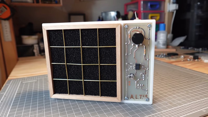
Nearly all modern PCBs are designed with the help of EDA software, but not all of them. [ALTco] shows us the process of plotting out a board the old-fashioned way — by hand.
Back in the day, drawing out the traces on a PCB lead to beautiful, smooth lines that [ALTco] wanted to imitate. But first, he needed to figure out how the rest of the fabrication process worked. He starts by just experimenting, both with the “resist” markers and paint, and the etching compound. Things rarely work first-try, and neither did his home-made etchant. So then it was time to buy some ferric chloride, the standard copper etchant for PBCs. A few more tests sorted out which permanent marker worked best.
[ALTco] starts by thoroughly cleaning a raw copper-clad board so the marker sticks properly, then draws the circuit for a little analog fan controller. The board is then laid in a bath of the etchant for several minutes while gently rocking it to keep the reaction going. Finally the board is taken out, etchant stored for re-use, and the board washed with water and then presumably IPA to remove the remaining marker. Some assembly of the newly-printed circuit board later and you have a cute little smoke absorber for your soldering projects.


Ok… try this… Rough the copper surface….
Use a 3D printer to lay out the PCB traces one pass high….
Think about it carefully.
Bad Obsession Motorsport on youtube invested far too much time and effort creating a system to effectively print traces direct onto a bare substrate!… On the one hand it’s impressive the lengths that they went to, on the other I’m sure that JLCPCB would have done multiple iterations in return for a favourable mention!
Ingenious! I’ve never considered this method. Does it actually work?
Maybe for fat traces, but I imagine undercutting would be a nightmare and any points with low adhesion would let etchant right in. That said I ain’t looked into it…maybe it’s a thing?
I have used in the past and got professional looking results with drafting tape you can buy various widths along with the IC pads and dot pads in general. I’ve cleaned the board using comet cleanser and then wash it with alcohol and then proceed to lay on your pattern with the tape and after you have it laid out I used an applique roller and rolled it out to make sure the adhesive is fully contacted so that the engine doesn’t crawl underneath. I use this method for prototyping as well as one off production boards for where I even worked. I’ve used FR4 and G4 fiberglass as well as the newer epoxy glass. I understand your issue using earn chloride but that works the best.
The method I’ve seen, used until 1990’s in Poland, used adhesive foil strips and circles to make the traces and solder pads, and then a lacquer made by dissolving rosin in methylated spirits, this concoction was loaded into syringe that had a small air hole on the side and bent needle for drawing. This was used for filling up spaces between foil strips. After etching and drilling and stripping off the foil the same mixture was used as protective solder mask. One benefit is that rosin was/is used in soldering as a natural flux…
The method I’ve been using back then was adhesive black strips and markers on transparent, and photo process to leave resist on a copper board, then engraved…
In 1990’s and 2000’s magazines that had DIY electronics projects in my country published PCB patterns on a dedicated page inside. There were two ways of using them. The cheap one was to make a good quality, high contrast Xerox copy and use that copy for thermal transfer. The expensive method used Positiv 20 photoresist on the PCB and either a few drops of oil or dedicated chemical spray to make paper insert more transparent. One could get an UV lamp for hardening resin nail polish, or use sun instead. The PCB was then placed in solution of ferric chloride for etching. There was also a chemical compound for coating the PCB in tin, but I think that rosin lacquer was cheaper and looked better.
I used to use vinyl cut stickers. I could reliably make tracks thin enough to go between IC pads.
Aaah old memories… back in the day I used these transparent transfer sheets, usually for lettering technical drawings but also were available with DIP pinouts and other common pads and traces. After rubbing and transferring the black to a PCB I could then use a masking pen to draw between the traces. Everything goes into the acid and alcohol would rub off the masking.
These transfer sheets also work great to create lettered front panels for projects. On any material panel, plastic, aluminum etc., paint the panel with the color you want for the lettering, say white. Transfer the letters onto it by rubbing the back of the transfer sheet. When complete, spray lightly over everything with the color of the panel you desire, say black. After it thoroughly dries, place tape over the lettering and pull off. The transferred letter with the black paint will come off revealing the white paint. Thus white letters on a black panel.
The word you’re looking for is Letreset. I used them long ago as my drawing skills only allowed me to draw breath and cash from an atm. I use those blue transfer sheets for my basic pcb’s. Stickers are made printing with an ink jet onto photo paper , sealing with aerosol lacquer, and fixing with double sided tape.
It’s “Letraset” https://en.wikipedia.org/wiki/Letraset
The branded sheets are collector’s items now, but many knock-offs exist and are available from your favourite stationery shop, graphics arts supply house or online bookseller.
Can you still get letraset pcb transfers? Steve
Double sided boards were laid out using tracks made from red and blue Rubylith tape, and black stickon labels for through hole ICs/connectors/etc.
Generally, after you had placed a track, you carefully avoided picking it up and moving it.
Yeah remember that. Puppets or something like.
I remember the transfer sheets and you could get rolls of black self adhesive crepe tape in varying sizes from 1mm to 4mm.😁
Hmmmm…. I can smell the etch resist pens and ferric chloride again…
I used to etch away as little copper as possible to make the FeCl last as long as possible. I discovered I could mask large areas using my Mum’s nail varnish – much cheaper than special etch resist pen!
You too?!
Here’s a still working example from 1973
https://entertaininghacks.wordpress.com/2015/02/21/a-40-year-old-hack-disinterred/
From an electrical point of view these traditional PCBs are sometimes better, even.
The hand-drawn curves used for traces have less reflection than perfectly geometric ones generated by circuit design software.
You can do curved / rounded traces with Kicad using the round traces plugin.
Reflection? RF?
True, but mostly irrelvant unless you are dealing with GHz signals.
https://www.signalintegrityjournal.com/articles/2104-should-you-worry-about-90-degree-bends-in-circuit-board-traces
https://www.simberian.com/AppNotes/Bends-AnalysisToMeasurements-2021-04-01.pdf
The short form:
It’s the capitance of the corner that matters, not the corner itself. If you make your corners such that the trace width is constant through the corner then you won’t have reflections. You don’t need artistically curved traces, just traces with the outside corner rounded at the bend. It is usually enough to simply chamfer the outer corner to approximate the trace width through the corner.
I bought a handmade guitar pedal to fix and resell. I opened it up to start fixing and the handmade pcb is so beautiful I don’t think I want to sell it anymore. I just want to hang it on the wall with the back cover removed and look at it. Who care if it works. It’s art!
I’m using sodium persulfate (B327), safer than ferric chloride.
Another option is ammonium chloride, which doesn’t stain.
My old-school process…
1. Draw layout on graph paper (usually 5×5 mm) with a pencil
2. Copy to parchment paper using a black ink pen. Needed to ink paper from both sides to be lightproof
3. Scrub copper of future PCB, then spray with photosensitive laquer (“Positiv 20” spray can)
4. Let dry at a completely dark place for 24 hours
5. Make a stack: laquered PCB, layout parchment, glass plate
6. Put under UV lamp for 10 minutes
7. Use NaOH solution to develop, rinse
8. Use warm ammonium persulfate solution to etch (much better than ferric chloride, does not leave dark stains everywhere).
9. Rinse and remove photo laquer using nitro thinner or similar
From time to time, I got the stack wrong by using the layout in the wrong direction (remember – always add some letters which must be readable…). This lead to bending all pins of DIP packages by 180 degrees then… and crossing C and E of TO-92 transistors :)
Good old times.
Pretty similar to what we used at school…
differences were that we:
* routed traces with some adhesive tape/stickers, typically at a bigger scale (2x, 3x)
* the photoresist material was not sprayed into the coper board, it was in sheet and laminated to the copper clad board, no 24h wait.
* the patern was projected (so scale could be adjusted) directly from the transparent.
* the cleaning of resist was done in some ultrasonic bath.
for the rest, really similar yes, including the warm ammonium persulfate.
we also had some roller based tinning machine to finish the boards nicely…
The process was rather quick, all in all, could have a board in half a day, the longest was clearly preparing transparents by hand… by the end they were starting to have software for that and some basic autorouter (some taking like 2h+ and failing in the end… sigh…) and printing unto transparent sheet
Superglue is your friend when placing those little parts.
That’s nice, but he shows himself babbling too much.
Nevermind, i’ve mixed up the videos.
At school, I made PCBs using this approach, but also using rub-on transfers for anything with a footprint (usually DIP sockets). Every time I’ve mentioned this to someone I’ve been getting blank looks. Did anyone else do this?
(Also, we had to colour in big slabs of copper for things like ground planes. This was done purely to save on etching fluid.)
Yes, the sheet had DIP pads but also circular component pads with a dot in the middle (to help centre the drill later), just join up with etch resist pen. I did this aged 13/14, around 1976/1977.
I even managed a double-sided PCB once, but had to drill the holes first for alignment of the two sides!
Nothing very fine by todays standards of course.
Helluva sense of achievement though. I made PCBs that way when I was 13 or so and just carried them around in my pocket for a few days, enjoying the huge step I’d made.
Letraset was the brand I used. My dad had an assortment of these. In 97 I discovered EAGLE and press-n-peel blue paper and everything changed forever.
That’s what I remember from the 80’s. Rub on transfers like letraset and resist tape for the trace lines. Resist pen for the weird angles and odd corners. I can still smell the ferric chloride.
That was one of my first “real” commercial jobs: Laying out boards using tape and press-on transfers on film. Sometimes at 2x size, then transferring with a reduction camera to lith film for production boards. For short-run stuff I’d lay out the tape on film at 1:1, and do a direct contact exposure on the board using a UV lamp from hell itself, then hand-etched in horrible ferric chloride etchant. Great job, great experience, would never go back.
I had one of those Rat Shack Ferric Chloride etching kits.
I’m positive that “etch resist pen” was just a Sharpie with the branding rubbed off.
The ink would always start running off before the copper was etched through. My traces always ended up a bit thin and pitted. It was still usable for simple circuits designed with thick traces that could afford to lose a little but I can’t imagine even getting a usable board for plain old 0.1″ (2.54mm) spaced dips and headers.
Later I tried cupric chloride. That worked a little better but still not well enough. I tried toner transfer next. So many old magazine articles and later internet posts made it seem like a perfect board via toner transfer applied with a plain old clothes iron should be a piece of cake. I had zero luck with the clothes iron. I ended up modifying a laminator to run hotter. That finally got me a board good enough to use an IC. But it still had pits in places and clearly looked amateur.
The one and only thing I ever tried that stuck to the copper all the way through the etching process and left a clean, no-pit, no-thinning copper surface underneath was nail-polish. But how much detail are you going to paint on with a nail-polish brush? Plus it was a PITA to clean it off afterwards.
Part of my problem.. it always seemed to take a LOT longer than every set of directions I ever read said it would to finish the etching. So.. more time to dissolve the resist.
But I tried all sorts of stuff for that too.
I broke half the blades off an old muffin fan to unbalance it and placed that under my etchant tank for vibration.
I put a heat lamp over it.
I even threw in a fish aerator.
That helped but not good enough.
Is everyone claiming to make decent PCBs at home lying or what?
I have had a pile of parts for several years that is supposed to become a CNC router for making PCBs. I just need to get my workshop cleaned out so I can start working on such things again….
Oh, and electrical tape. That seems to work good. But just how complex of a circuit and how narrow of traces am I going to cut out of a piece of electrical tape? For the really simple stuff I’ll just use stripboard and anything more seems too complex to bother with that method.
This has brought my wife’s Cricut machine to mind… but again… for a board complex enough to bother the ‘picking’ would be ridiculous.
If you have access to a Cricut, there’s this: https://www.reddit.com/r/electronics/comments/914oa4/singlesided_copper_pcb_cut_with_a_cricut_cutting/
(From the comments on this recent HaD article: https://hackaday.com/2026/05/19/using-3d-printers-to-make-circuit-boards/#comments )
I had similar experiences with laminating resist onto the board and with ferric chloride. But cnc routers for doing quick run pcb’s are awesome once you spend the large amount of time required to get them aligned and cutting the right depth through somewhat variable thickness copper. (All the ones I’ve used rely on V shaped cutters so cutting depth and trace width are inversely related, and local variations in board height/warp and copper thickness result in trace width issues.) But they’re fast, pretty clean, and double sided boards with vias are easy.
Toner transfer only works well with an old analog photocopier with the darkness cranked way up.
Newer copiers and printers don’t use enough toner. The trick to getting toner transfer to work with a laser printer was to apply Pulsar foil after the transfer. It would only stick to the toner and seal it up. Unfortunately they seemed to have discontinued the stuff. There are other brands of toner reactive foil available, but they are for decorative purposes and I don’t know if it would work as an etch resist.
Toner transfer definitely works with modern laser printers. About 12 years ago I used my Samsung SCX-4300 to make two-sided PCBs.
First, make sure to check your prints for X and Y distortion. In my case the Y (A4’s 297 mm) was fine, but X (A4’s 210 mm) had to be rescaled with a factor of 101,2% for dimensions on screen and in print to match.
Rookie mistake – do NOT print PCB layers as raster images (like directly from EAGLE). Their quality will indeed suck because they are somehow processed by printer’s own SoC.
Now for the actual process of PCB printing.
You must use glossy photo paper so that toner will happily leave it and stick to copper when heated. Maybe glossy magazine paper would also work but I didn’t test it.
I forgot exact details but I think I saved my EAGLE board top and bottom layers as PDF. (Or maybe I used PDF printer? I think it was “save” function though.)
PDFs with PCB layers were imported into Adobe Illustrator. I added registration marks – simply very fine horizontal and vertical lines about 5 cm away from actual board image. Those will help me align both printouts before doing toner transfer.
Here’s the most important trick. When I did my printing with Adobe Illustrator, the printer probably receives PostScript / vector data and board printouts come out razor-sharp with a thicc layer of toner. Even doing tiny traces for tiny 0402 components was not a major issue back then. (Of course in Adobe Illustrator print dialog I also applied the X scaling factor. Adobe Reader might not support that option.)
However, if I did my printing as a regular raster image (PNG or BMP) the printer probably receives bitmap data, reinterprets it internally and resulting prints are not as fine (which is VERY important for PCB work).
I don’t know exactly what happens in the printer’s firmware but I suppose laser is driven somewhat different when print is made out of vector data instead of raster images.
I would align my top and bottom printouts and secure them on three sides with masking tape – because it doesn’t melt when in contact with hot surfaces. It would make something that looks like a pocket.
Right before doing toner transfer, two sides of the board had to be gently scrubbed with soapy water and wet grade 1000 sandpaper. Then degreased with acetone.
After cleaning, I would put my board-to-be into this “pocket” made out of two bits of glossy paper. I would heat it with regular clothes iron on both sides. I think I also used to apply a bit of pressure with a small, crumbled rag while the board and paper was still hot from ironing. This improved toner transfer and prevented broken traces.
I would cut the tape if it didn’t unstick itself already from the heat. I left the board to cool down. After it’s cooled, it went into a water bath (or maybe soapy water bath, don’t remember) for about 15 minutes. The glossy photo paper would get wet and come out by itself while toner would remain stuck to the copper.
After rinsing it in water and removing any paper residues (unlikely, but happened sometimes), the board went into ferric chloride bath for about… 20 minutes? I inspected it every few minutes to check how it goes and to shake FeCl bath. After determining that it’s fully etched, I would rinse it with water and remove toner using paper towel soaked in acetone.
And there it is. A brand new 2-layer PCB done at home. Now it’s time for drilling all the holes with Proxxon drill and 0,3 mm or 0,5 mm carbide drill bits; and finally to solder components.
I had this process perfected during my student years as procrastination often led to building robot PCBs right on the night before competition – and in such case the failure (and resulting waste of time) is not an option.
Also, using quality boards from TME helped immensely. Boards from a local store were slightly cheaper, but were made out of pure chinesium. Despite cleaning, toner wouldn’t stick, there were issues with copper thickness, under and over etched parts of the print. Utter mess.
The problem I have is toner density. The toner fully transfers to the board and sticks fine, but there just isn’t enough. The printer is set to its darkest setting, but I can see copper through the toner and the surface comes out very pitted. I’ve tried 3 different printers with the same results.
If I use the Pulsar foil, it seals up the little holes and the board comes out perfect. Unfortunately it has been discontinued. I will probably have to switch to photoresist when I run out of foil. I never had good luck with the dry film, it always arrived damaged. I haven’t tried the liquid stuff yet though.
“I’m positive that “etch resist pen” was just a Sharpie with the branding rubbed off.”
Decon Dalo (?) pens definitely weren’t the same.
They contained a thick blue liquid and had a valve in the pen. Push the pen to get more ink out – flooding out in a puddle :( Dreadful things, so I (re)invented other etch resists.
I used to find it virtually impossible to get some chemicals when I was younger. Ferric chloride being one of those. So I used to make my own.
Let copper sulphate react with some iron nails, to make iron sulphate, then use table salt and electrolysis to make the iron chloride solution. Iron or D battery carbon rods were my way to go rather than producing the chlorine using bleach and vinegar because the bleach had other things mixed in with it. I’d also make my own copper sulphate if I couldn’t get any from local farmers, you never got a huge amount in chemistry sets.
Mac?
Same.
But not etchant, that was easy.
You’d be amazed at the number of busy bodies that won’t sell a 12 YO fuming nitric acid.
You can concentrate acids at home…
Dad corrected me, sent me to the reloading isle at the gun store.
Still have an above average # of fingers.
I used a sharpie, after discovering that the Radio Shack etch resist pen seemed to be a rebranded sharpie. Once the etching was complete I removed the pen ink with kitchen abrasive cleanser (Comet, Bon Ami, etc.)
Red Staedtler(lumocolor?) was great – but pricey(you could buy eight to twelve bottles of cheapest nail polish for same money).
Rapidograph filled with a alcohol based lacquer(even diy from shellac or colophony rosin) was nice for fine details, but claening/rinsing it afterwards(and better be quick!) was pure horror…
Removing the sharpie ink is important. Sharpie ink is acidic to improve adhesion, and it will etch the copper a little.
If I only needed to make one small board. A knife and a file. Otherwise resist pen and rubbed transfer decals. Often patch wires if the resist pen didn’t work in spots. Later my friend got a laser printer that could lay down thick toner and just transfer the whole thing. It didn’t save time for something simple but looked was nicer.
I remember doing this in the 90s with a RadioShack kit. Had to drill out the holes with a dental drill.
This is the exact way they taught us at school. We had to make our first few PCBs this exact way. If we were successful, we could move on a laser printer and old steam iron with no steam setting. That’s how we finished school.
I don’t consider this a hack as it was simply the way to make PCBs yourself back in the day.
There were even rub off stencils for ic-footprints and a good permanent marker does a good job for traces. I did quite a lot of those in the 80’s but it was never my favorite thing to do.
How many nights have I spent doing my own boards with a permanent marker and a 1.5 mm drill bit …. I really enjoyed those years!
I still have some Bishop Graphics tape and rub-on transfer patterns in the basement from long, long ago. I spent too many hours with them back in the day :-)
Old? Even here, where I live, most PCB prototypes, even individual commercial ones, still use this manual etching method. The etching process is still taught/used in schools, although digital methods have begun to be introduced.
ignorant here but I can’t help reading IPA to clean as being India Pale Ale.
I assume that is not to improve the taste of that drink….