
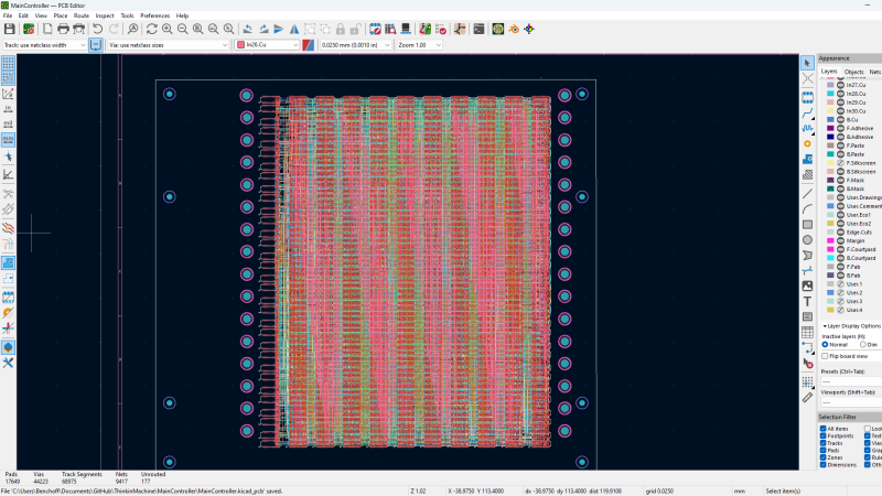
[Brian] had an absolute monster of a PCB with thousands of nets to be routed, the kind of design that stopped traditional routers in their tracks. It would take months to route by hand, likely trying the patience of a saint in the process. To solve this specific problem he created OrthoRoute, a GPU-accelerated autorouter that he cautions is no more trustworthy than any other autorouter, but at least it’s fast!

A KiCad plugin, OrthoRoute is so named because traces are laid down in a Manhattan lattice, a grid of orthogonal segments. All components (surface-mount only, no through-hole stuff) go on the top layer of the PCB, and all lower levels contain a grid of traces, connected as needed with blind and buried vias to route everything. OrthoRoute takes a structured and iterative approach, eventually converging on a satisfactory layout.
How does OrthoRouter actually decide how to connect things? [Brian] adapted PathFinder, an algorithm designed for routing FPGAs. Laying out a grid of orthogonal traces and punching down through them with vias to make connections has a lot in common, conceptually, with routing FPGAs. GPU acceleration makes the whole thing far more efficient than pipelining the calculations through a CPU.
OrthoRoute was built to solve a very specific problem, but in the process showed that GPU-accelerated routing is definitely feasible. Check it out in the videos, embedded below the page break.
[Brian] cautions that as-is, OrthoRoute is useful to maybe a handful of people at best, but as a KiCad plugin it’s highly modular and the hard parts are all done. If you want a closer look, or have some ideas about how to repurpose or extend it, check out the GitHub repository.
We’ve seen some nifty KiCad plugins for all kinds of purposes, from breadboarding to giving PCB traces an old-timey look, and even one specifically for designing custom keyboards. It’s not every day we see a plugin aimed at handling high-density boards with thousands of nets, though.










For decades, Cadence and others have had autorouters capable of much more complex designs than this.
Nonetheless I regard this as a significant accomplishment. I’ve looked at the theory behind autorouters, and my mind just won’t translate the theory into code.
Really?
What algorithm are they using, because this fairly quickly becomes NP complete, which means the solution is to brute force it in on way or the other.
To very little surprise, most of that algorithmic knowledge is proprietary. Note that while the (multi)planar graph embedding problem is NP in most cases, that doesn’t mean that heuristics don’t function at all; you’ll find that in virtually all routing and layouting programs, you never start within a framework such that only the optimal solution would be accepted, but one where you can get iteratively closer to a good solution. And that’s fair, because you rarely gain much by provable optimality, and much more by attainable OKish-ness.
No brute force is guaranteed to take ages (when it is NP complete, which it is). You need a heuristic that performs reasonably.
Dear,
Nice idea and first simple results.
Such kind of routing was already available early 80’s to handle 74xxx/40xxx based digital boards.
Would like to see real complex PCB design wit embedded SOC/FPGA, medium size BGA, DDRx SOC and FPGA memory interfaces. Track length and impedance controlled [lauers] matching with/without via’s.
Super cool, can’t wait to give this a go!
Nobody is asking the real question here: What do those 1100 pin connectors look like and what are these used for?
This will be an expensive board to manufacture and with 32 layers a thick one too.
I think the first picture of the blog post answers that. A double-row of 2×11 connectors, 50 positions each. These look like mezzanine or board-edge connectors; given the placement, the latter.
And of that, 16 double-rows.
A “really complex backplane”, to cite the README.md .
So, backplane with really many signals. Probably a massive sensor array or controller array thing, at non-negligible, but also not at extreme bandwidths (the large amount of layer crossings would cause a lots of problems of the emissive and crosstalk kind were you to route, say, PCIe 5 across these).
Also, constrained in vertical space, and still somewhat constrained in cost, since Brian didn’t pick ANSI/VITA 41.0/46/46/78 connectors, and that probably for a reason.
Massively so, yes, the number of vias will also drive tooling and production time costs, and probe testing will take forever, so it’s likely it’ll mostly be done as a sampling.
It’s not a real board. It’s just a test case for the auto router.
And apparently there are more options for autorouters in KiCad. See the link below.
https://forum.kicad.info/t/options-for-autorouters/70029
The thread above (probably) got started as a response to a modernization attempt of freerouting, which stranded in vagueness about licencing issues around freerouting.
https://forum.kicad.info/t/freerouting-modernization/69547
Why would you say that it’s a “test case”?
It’s an obviously absurd breakout board, and if there’s one thing I know about Brian Benchoff, it’s that he’s deadly serious about absolutely absurd.
Mark my words. I don’t know what it is, but it’s going to be cool. Or at least excessive. :)
I applaud the ingenuity to write an autorouter and make it work. Impressive accomplishment really.
I know it is a test case..
But on the system level, I would be more interested in resolving and simplifying the weird board in the first place. That many pins, zig zag all over the place without signal integrity concerns? Only slow analog? (then please digitize them) or slow digital? Led breakout? (put a microcontroller and do it in software)
Maybe retro computing, replacing a failed module? (maybe scan the original, that seems to require many layers)
If you have that many nets, chances are you need signal integrity, or even differential pairs.
Why they recommends expensive H100 GPUs instead of RTX 6000?
Using an H100 is notional. If you read the rest of the Github repository README, you’ll see that this supports a number of GPUs, depending on how complex your routing is:
Board Size Layers Grid Pitch Nodes VRAM Needed GPU Required
100×100mm 6 0.4mm 375k 8-12 GB RTX 3080, RTX 4070
150×150mm 18 0.4mm 2.53M 18-24 GB RTX 4090
200×200mm 18 0.4mm 4.5MM 24-30 GB RTX 6000 Ada (48GB)
200×200mm 32 0.4mm 8M 35-40 GB A100 80GB, H100
300×300mm 32 0.4mm 18M 60-80 GB H100 80GB
There is a 60/70s era of IBM mainframe boards designed on the opposite concept – everything is THT, even the free space is filled with vias – so this forms an uniform grid. No expensive blind/burried vias. Then the routing goes likely manhattan style X/Y on alternate layers, between the throuh hole pads, unless they are used for layer change. Its pretty neat and definitely automated design could have been used for that.
The first one of those I saw was a main storage card for a stat-mux, (Statistical Multiplexer – a sort of router for IBM proprietary networks).
Which I thought it had been built on perf-board :)
Notting special since autoroutig 74xxx/40xxx TTL/CMOS based ciruits designs where already done in the 80’s. If one can adapt the presented tool to handle complex BGA based designs based upon System On Chip, BGA FPGA, DDRx components and lenght matched, impedance controlled constrained routing then I’m interested.
Could you auto route a lattice and place magnetic memory (like) construction or a type of material that would allow for mangnitc beads like memory?