RPDot: The RP2040 Dev Board Barely Bigger Than The Chip

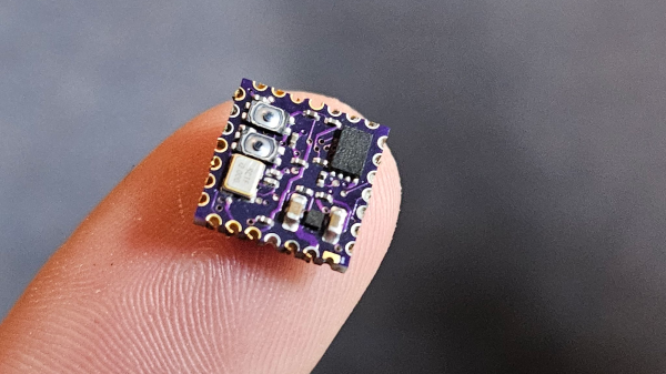
Is [William Herr]’s RPDot actually the world’s smallest RP2040 dev board? We can’t say for sure, but at 10 mm on a side, we’d say it has a pretty good shot at the record.

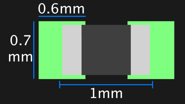
Not that it really matters, mind you — the technical feat of building a fully functional dev board that’s only 3 mm longer on each side than the main chip is the kind of stuff we love to see. [William] says he took inspiration from the [SolderParty] RP2040 Stamp, which at one inch (25.4 mm) on a side is gigantic compared to the RPDot. Getting the RP2040 and all the support components, which include an 8MB QSPI Flash chip, a 3V3 LDO, a handful of 0201 passives, and even a pair of pushbuttons, required quite a lot of design tweaking. He started his PCB design as a four-layer board; while six layers would have made things easier, the budget wouldn’t allow such extravagance for a prototype. Still, he somehow managed to stuff everything in the allotted space and send the designs off — only to get back defective boards.

After reordering from a different vendor, the real fun began. Most of the components went on the front side of the board and were reflowed using a hot plate. The RP2040 itself needed to go on the back side, which required gentle hot air reflow so as not to disrupt the other side of the board. The results look pretty good, although those castellated edges look a little worse for the wear. Still, for someone who only ever worked with 0402 components before, it’s pretty impressive.

[William] says he’s going to open-source the designs as well as make some available for sale. We’ll be looking out for those and other developments, but for now, it’s just pretty cool to see such SMD heroics.

A graphic showing the suggested footprint dimensions for 0402 parts

Want Better 0402 Reflow? Consider These Footprints!

Assembling with a stencil is just that much more convenient – it’s a huge timesaver, and your components no longer need to be individually touched with a soldering iron for as many times as they have pads. Plus, it usually goes silky smooth, the process is a joy to witness, and the PCB looks fantastic afterwards! However, sometimes components won’t magically snap into place, and each mis-aligned resistor on a freshly assembled board means extra time spent reflowing the component manually, as well as potential for silent failures later on. In an effort to get the overall failure rate down, you will find yourself tweaking seemingly insignificant parameters, and [Worthington Assembly] proposes that you reconsider your 0402 and 0201 footprints.

Over the years, they noticed a difference in failure rates between resistor&capacitor footprints on various boards coming in for assembly – the size and positioning of the footprint pads turned out to be quite significant in reducing failure rate, even on a tenth of millimeter scale. Eagle CAD default footprints in particular were a problem, while a particular kind of footprint never gave them grief – and that’s the one they recommend we use. Seeing the blog post become popular, they decided to share their observations on 0201 as well, and a footprint recommendation too. Are your 0402 resistors giving you grief? Perhaps, checking the footprints you’re using is a good first step.

The 0402 and 0201 components are in a weird spot, where soldering iron assembly is no longer really viable, but the stencil+reflow approach might not be unilaterally successful when you start off – fortunately, that’s where writeups like these come in. Interested in learning stenciling? Get some solder paste, and read up on all the different ways you can put it onto your boards.