I recall the point I started taking electronics seriously, although excited, a sense of dread followed upon the thought of facing the two main obstacles faced by hobbyists and even professionals: Fabricating you own PCB’s and fiddling with the ever decreasing surface mount footprints. Any resistance to the latter proves futile, expensive, and frankly a bit silly in retrospect. Cheap SMD tools have made it extremely easy to store, place, and solder all things SMD.
Once you’ve restricted all your hobbyist designs/experiments to SMD, how do you go about producing the PCBs needed for prototyping? Personally, I dread the thought of etching my own boards. The process is laborious and involves messy chemicals and specially sensitized PCB’s — none of which interest me. I’ve only ever done it a few times, and have promised myself never to do it again. Professional but cheap PCB manufacturing is more like it board pooling services such as OSH park have made this both easy and affordable — if you can wait for the turnaround.
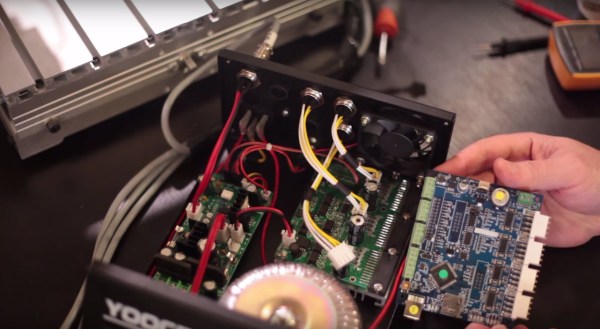
So what are the alternatives? If you are really serious about swift prototyping from your own Lab, I put forth the case of milling your own PCB’s. Read on as I take you through the typical workflow from design to prototype and convince you to put up with the relatively high start up cost of purchasing a PCB mill.


