Reprogrammable Transistors

Not every computer can make use of a disk drive when it needs to store persistent data. Embedded systems especially have pushed the development of a series of erasable programmable read-only memories (EPROMs) because of their need for speed and reliability. But erasing memory and writing it over again, whether it’s an EPROM, an EEPROM, an FPGA, or some other type of configurable solid-state memory is just scratching the surface of what it might be possible to get integrated circuits and their transistors to do. This team has created a transistor that itself is programmable.

Rather than doping the semiconductor material with impurities to create the electrical characteristics needed for the transistor, the team from TU Wien in Vienna has developed a way to “electrostatically dope” the semiconductor, using electric fields instead of physical impurities to achieve the performance needed in the material. A second gate, called the program gate, can be used to reconfigure the electric fields within the transistor, changing its properties on the fly. This still requires some electrical control, though, so the team doesn’t expect their new invention to outright replace all transistors in the future, and they also note that it’s unlikely that these could be made as small as existing transistors due to the extra complexity.

While the article from IEEE lists some potential applications for this technology in the broad sense, we’d like to see what these transistors are actually capable of doing on a more specific level. It seems like these types of circuits could improve efficiency, as fewer transistors might be needed for a wider variety of tasks, and that there are certainly some enhanced security features these could provide as well. For a refresher on the operation of an everyday transistor, though, take a look at this guide to the field-effect transistor.

Laser doping silicon wafer

Laser Doping His Way To Homemade Silicon Chips

It’s a pity that more electronics enthusiasts haven’t taken the hobby to its ultimate level: making your own semiconductors. There are plenty of good reasons for that: chief among them is the huge expense involved in obtaining the necessary equipment. But for the sufficiently clever, there are ways around that.

[Zachary Tong] is dipping his toes into the DIY semiconductor world, and further to the goal of keeping costs to a hobbyist scale, is experimenting with laser doping of silicon. Doping is the process of adding impurities to silicon wafers in a controlled manner to alter the electrical properties of the semiconductor. [Zach]’s doping method is a more localized version of the simple thermal diffusion method, which drives a dopant like phosphorus into silicon using high temperatures, but instead of using a tube furnace, he’s using a fiber laser.

The video below shows his two-step process, which first blasts the silicon oxide layer off the wafer before doping with the laser shining through a bath of phosphoric acid. The process is admittedly fussy, and the results were mixed at best. [Zach]’s testing seems to suggest that some doping occurred, and it even looks like he managed to make something reasonably diode-like using the method.

Although the jury is still out on [Zach]’s method, we thought the effort was the important bit here. Granted, not everyone has a fiber laser kicking around to replicate his results, but it’s always good to see progress in the DIY semiconductor field. Here’s hoping [Zach]’s work, along with the stuff that [Sam Zeloof] is doing, kicks off a spate of garage semiconductor fabs.

Continue reading “Laser Doping His Way To Homemade Silicon Chips”

Fun With A 200-kW Fiber Laser

We’ve all heard the “Do not stare into laser with remaining eye” joke. It’s funny because it’s true, as pretty much any laser a hobbyist can easily come by can cause permanent damage to eyes unless the proper precautions are taken. But a fiber laser with 200kW peak power is in another hazard class entirely.

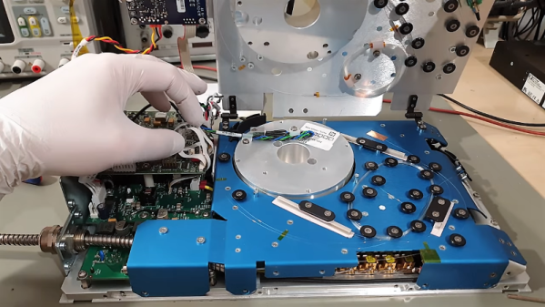
Granted, outsized power ratings like this are a bit misleading, based as they are on femtosecond-long pulses. And to be sure, the fiber laser that [Marco Reps] tears down in the video below was as harmless as a kitten when he got it, thanks to its output optics having been unceremoniously shorn from the amplifier by its former owner. Reattaching the output and splicing the fiber would be necessary to get the laser lasing again, but [Marco] had other priorities in mind. He wanted to understand the operation of a fiber laser, but the tangle of fibers on two separate levels inside the chassis was somewhat inscrutable. The coils of fiber wrapped around the aluminum drums inside the chassis turned out to be the amplifier; fed by a semiconductor seed laser, the light pulse travels through the ytterbium-doped fiber of the two-stage amplifier, which is the active gain medium where stimulated emission, and therefore amplification, occurs.

With a little reverse engineering and the help of an online manual, he was able to understand the laser’s operation. A laser company helped him splice the optics back together – seeing the splicing rig in action is worth the price of admission alone – and the unit seems to be in more or less working order at this point. Normally the most powerful laser we see around here are the CO2 lasers in those cheap Chinese laser cutters, so we’re looking forward to learning more about fiber lasers.

Continue reading “Fun With A 200-kW Fiber Laser”