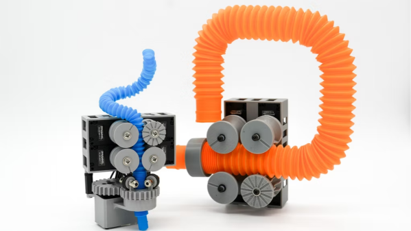
Are you familiar with pop tubes? Resembling the corrugated section of a bendy straw, they are at the core of PopTuber, an intriguing research project from the Actuated Experience Lab at the University of Chicago.
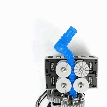
PopTuber shows how five motors and some specialized gears are all it takes to bend pop tubes into complex and stable 3D shapes. One can design the shapes in software, feed a pop tube into the shaper, and watch the device do the work. Importantly, the device can just as easily reset and re-use the tube. Watch the video (embedded below the page break) to see it in action and get a feel for what it can do.
In concept, it’s a little like a wire-bending machine, although wire benders are bulkier in comparison, more complex to scale, and unbending a wire is a separate process with its own hardware.
This project explores possibilities for a machine that can crank out complex curves on demand, such as oddball user interfaces, physical prototyping, and even a strange sort of physical display. But the real forward-thinking and interesting question researchers asked is whether this idea could be a form of programmable matter. The project shows that five actuators in a relatively compact package are all that’s needed to shape (and reset) a pop tube of arbitrary length in a programmable way, and it can scale easily to different sizes.