Depositing Metal On Glass With Fiber Laser

Fiber lasers aren’t nearly as common as their diode and CO2 cousins, but if you’re lucky enough to have one in your garage or local makerspace, this technique for depositing thin films of metals in [Breaking Taps] video, embedded below, might be worth checking out. 

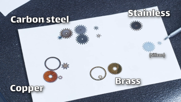
It’s a very simple hack: a metal shim or foil is sandwiched between two pieces of glass, and the laser is focused on the metal. Etching the foil blasts off enough metal to deposit a thin film of it onto the glass.  From electron microscopy, [Breaking Taps] reveals that what’s happening is that microscopic molten metal droplets are splashing up to the ̶m̶e̶t̶a̶l̶  glass, rather than this being any kind of plasma process like sputtering. He found this technique worked best with silver of all the materials tested, and there were a few. While copper worked, it was not terribly conductive — he suggests electroplating a thicker layer onto the (probably rather oxidized) copper before trying to solder, but demonstrates soldering to it regardless, which seems to work. 

This might be a neat way to make artistic glass-substrate PCBs. More testing will be needed to see if this would be worth the effort over just gluing copper foil to glass, as has been done before. [Breaking Taps] suspects, and we agree, that his process would work better under an inert atmosphere, and we’d like to see it tried.

One thing to note is that, regardless of atmosphere, alloys are a bit iffy with this technique, as the ‘blast little drops off’ process can cause them to demix on the glass surface. He also reasons that ‘printing’ a large area of metal onto the glass, and then etching it off would be a more reliable technique than trying to deposit complex patterns directly to the glass in one go. Either way, though, it’s worth a try if you have a fiber laser. 

Don’t have a fiber laser? Maybe you could build one. 

Continue reading “Depositing Metal On Glass With Fiber Laser”

Fiber Laser Your Way To Flexible PCB Success!

It’s not often we feel that something we’re featuring is a genuinely new and groundbreaking technique, but a team from the University of Maryland’s Small Artifacts Lab may have done just that with their foldable and flexible PCBs created using a fiber laser engraver.

Laser engraving a PCB is nothing new, but they’ve taken a custom PCB material made using Kapton tape and copper foil, and fine-tuned the engraver to not only selectively remove copper, but also to create in-place folds in the Kapton substrate. They have even used the laser to melt solder paste and solder components, though we’re not so convinced about the quality as seen in the video below the break. This means that they can not only create 3-dimensional PCB sculptures but also useful structures such as their example of an all-PCB micro switch. To make things easy they’ve even created a custom CAD package for designing in this medium.

Perhaps best of all, there appears to be nothing here that couldn’t be also performed outside the lab by anyone with enough Kapton and copper, and a fiber laser. We’re looking forward to where this technique will go. If you’re interested, you can read their paper here.

Continue reading “Fiber Laser Your Way To Flexible PCB Success!”

Micromachining With A Laser

[Breaking Taps] has a nice pulsed fiber laser and decided to try it to micromachine with silicon. You can see the results in the video below. Silicon absorbs the IR of the laser well, although the physical properties of silicon leave something to be desired. He also is still refining the process for steel, copper, and brass which might be a bit more practical.

The laser has very short duration pulses, but the pulses have a great deal of energy. This was experimental so some of the tests didn’t work very well, but some — like the gears — look great.

Continue reading “Micromachining With A Laser”