The 2022 Hackaday Prize is on, and we’ve already seen some incredible submissions by folks who believe their idea just might have what it takes to make the world a better place. But as with all contests, it’s good to understand all the rules before you get too involved. We promise nothing’s hidden in the fine print, but we certainly don’t fault anyone who wants to make sure.
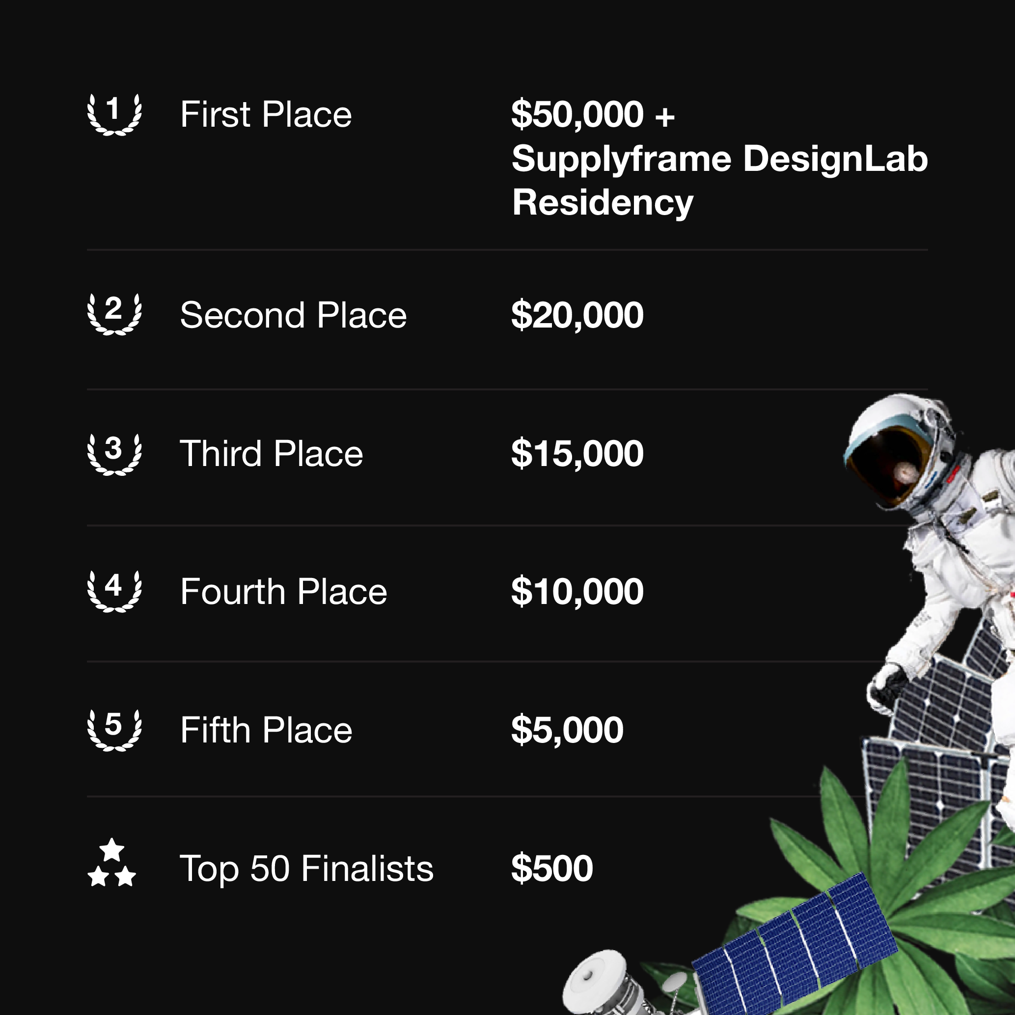
Which is why Majenta Strongheart, Head of Design and Partnerships at our parent company Supplyframe, stopped by this week’s Hack Chat to answer any and all questions the community had about this global hardware design challenge. A lot of ground was covered in an hour, with Majenta making sure everyone’s questions and concerns were addressed to their satisfaction. After all, with a residency at the Supplyframe DesignLab and a total of $125,000 in prize money up for grabs, we want to make sure everyone’s got the facts straight.
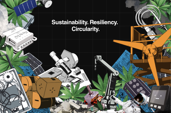
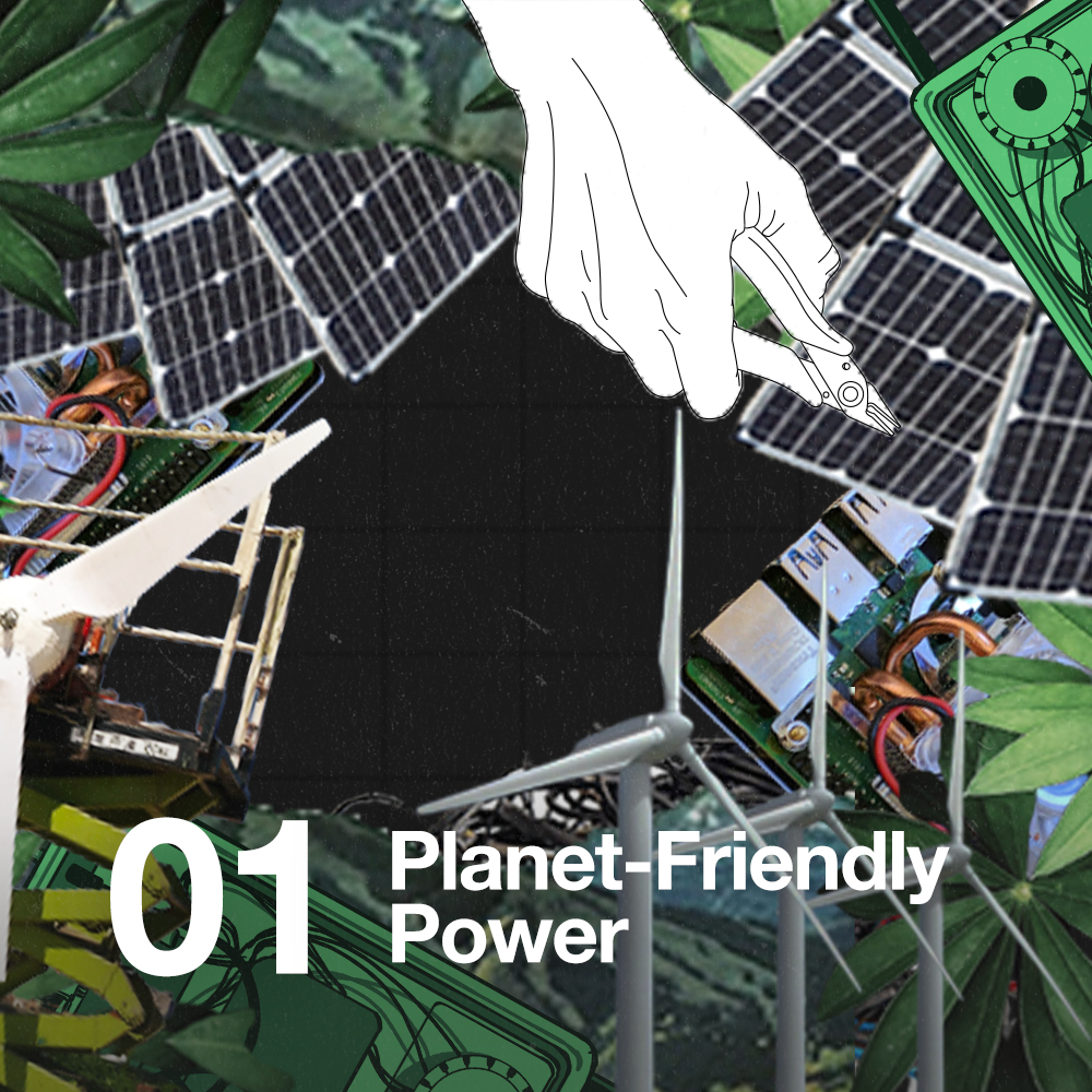
 So what burning questions did the Hackaday community have about this year’s Prize? Several people wanted to know more about the themes of sustainability, circularity, and climate crisis resiliency. For example, what exactly does circularity mean in this context? While Challenge #2 “Reuse, Recycle, Revamp” most clearly exemplifies the idea, Majenta explained that this time around the judges will be giving particular consideration to ideas that limit the extraction of raw materials and the production of waste.
For a practical example, 2022 Hackaday Prize judge James Newton pointed to the direct granule extruder designed by Norbert Heinz. The project, which took 5th place last year, allows waste plastic to easily be repurposed in a desktop 3D printer. This includes objects which the printer itself produced, but for whatever reason, are no longer desired or needed. This “life-cycle” for printed objects, wherein the same plastic can be printed over and over again into new objects, is a perfect encapsulation of circularity within the context of this year’s prize.
Others were looking for clarification on the contest rules. Specifically, there was some confusion about entering existing projects into the competition. Did it have to be a completely new idea? What if you’d already been working on the project for years, but had never shown it publicly before? Not to worry — existing projects can absolutely be entered into the 2022 Hackaday Prize. In fact, even if the project had already been entered into the Hackaday Prize previously, it’s still fair game.
 But there is an important caveat: to be eligible for this year’s Prize, the project MUST be documented on a new Hackaday.io page. Additionally, if it’s a project that has previously been entered into a Hackaday contest, you’ll have to show that it is “significantly different from when previously entered and show meaningful development during the course of the Contest“, as stated in the official rules. In layman’s terms, it means that anyone who tries to submit and old and outdated Hackaday.io page into the competition will find their entry disqualified.
Towards the end of the Chat, Erin Kennedy, a Hackaday Prize veteran that readers may know better as “Erin RobotGrrl” brought up the subject of mentors. In previous years, hardware luminaries like Andrew “Bunnie” Huang and Mitch Altman were made available to offer advice and guidance to the individuals and teams behind the Prize entries. While very proud of this effort, Majenta explained that at least for now, Mentor Sessions are on hold until that aspect of the program can be retooled. The main issue is figuring out the logistics involved; planing video calls between several groups of busy folks is just as tricky as it sounds. That said, bringing the Mentor Sessions back for 2022 isn’t completely out of the question if there’s enough interest from the competitors.
We appreciate Majenta taking the time to directly answer questions from the community, and hope that those who had their questions or concerns addressed during the Chat will ultimately decide to toss their hat into the ring. With a worthy goal and plenty of opportunities to win, we sincerely want to see as many people as possible get their entries in before the October 16th deadline. If you’re ready to take the next step, head over to the Contest page and show us what you’ve got.
The Hack Chat is a weekly online chat session hosted by leading experts from all corners of the hardware hacking universe. It’s a great way for hackers connect in a fun and informal way, but if you can’t make it live, these overview posts as well as the transcripts posted to Hackaday.io make sure you don’t miss out.