If you’ve done any amount of electronic design work, you’ll be familiar with the need for decoupling capacitors. Sometimes a chip’s datasheet will tell you exactly what kind of caps to place where, but quite often you’ll have to rely on experience and rules of thumb. For example, you might have heard that you should put 100 µF across the power supply pins and 100 nF close to each chip. But how close is “close”? And can that bigger cap really sit anywhere? [James Wilson] has been doing research to get some firm answers to those questions, and wrote down his findings in a fascinating blog post.
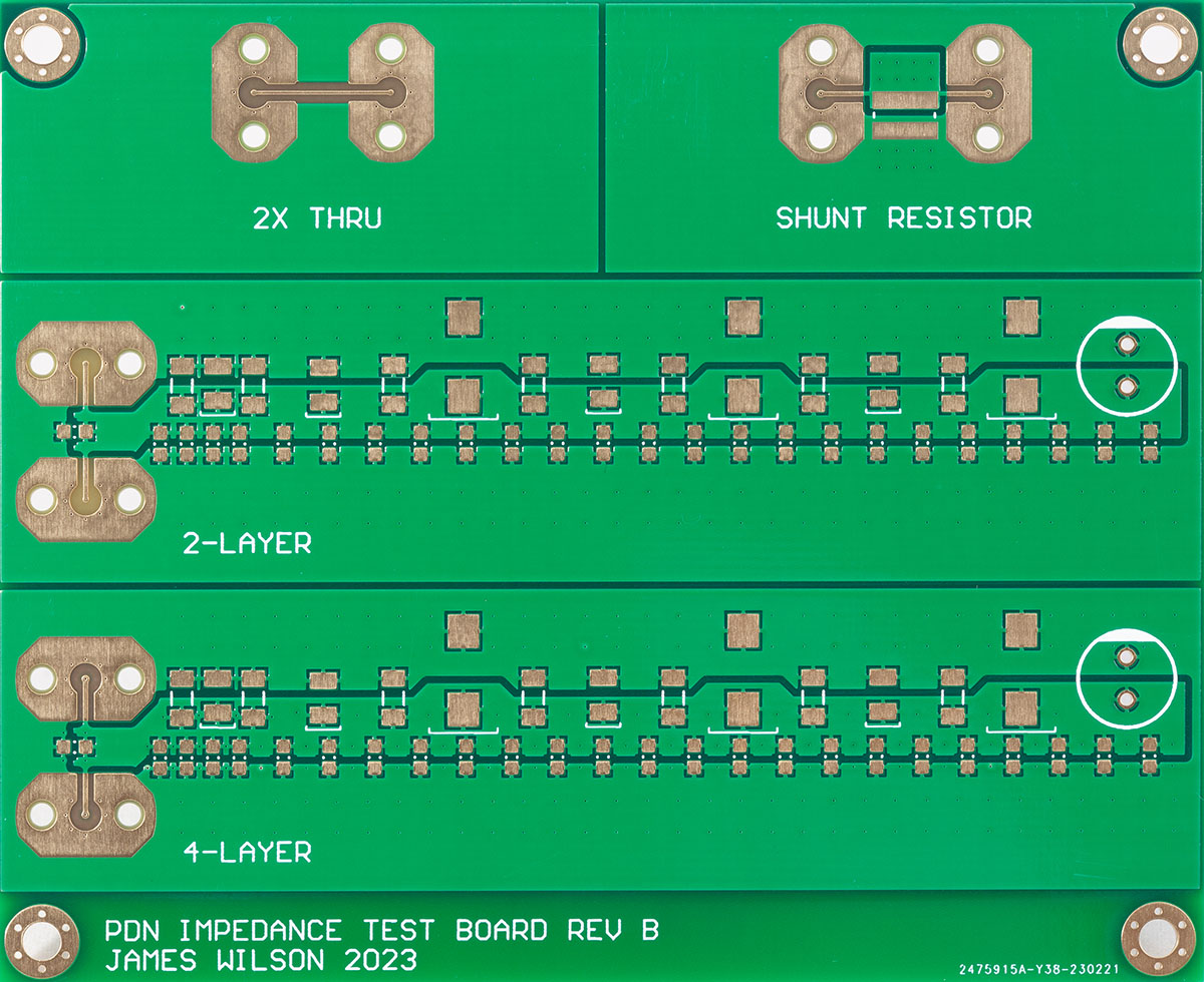
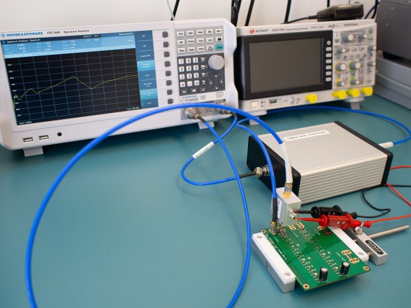
[James] designed a set of circuit boards that enabled him to place different types of capacitors at various distances along a set of PCB traces. By measuring the impedance of such a power distribution network (PDN) across frequency, he could then calculate its performance under different circumstances.
The ideal tool for those measurements would have been a vector network analyzer (VNA), but because [James] didn’t have such an instrument, he made a slightly simpler setup using a spectrum analyzer with a tracking generator. This can only measure the impedance’s magnitude, without any phase information, but that should be good enough for basic PDN characterization.
The results of [James]’s tests are pretty interesting, if not too surprising. For example, those 100 nF capacitors really ought to be placed within 10 mm of your chip if it’s operating at 100 MHz, but you can get away with even 10 cm if no signals go much above 1 MHz. A bulk 100 µF cap can be placed at 10 cm without much penalty in either case. Combining several capacitors of increasing size to get a low impedance across frequency is a good idea in principle, but you need to design the network carefully to avoid resonances between the various components. This is where a not-too-low equivalent series resistance (ESR) is actually a good thing, because it helps to dampen those resonances.
Overall, [James]’s blog post is a good primer on the topic, and gives a bit of much-needed context to those rules of thumb. If you want to dive deeper into the details of PDN design or the inductance of PCB traces, our own [Bil Herd] has made some excellent videos on those topics.


