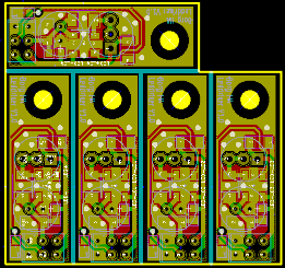
Kicad Symbol Generating Script Shows Promise

Kicad is a fantastic PCB layout tool. We think creating a part for use with Kicad is in many ways easier than in Eagle, but it never hurts to have a few shortcuts. Here’s a new way to quickly get your parts into the schematic editor. It’s a Python script that generates symbols from an XML input file. You create the XML file with a list of all the pins on your part and the function they will serve. The Python script will then format that as a library file which can be imported by Kicad.

It’s a little bit clunky due to the number of steps in the process. But it is possible to use a CSV file generated in a spreadsheet program to create the XML needed by the script. We’ve used the online component builder ourselves, and appreciate the possibility of mass pin assignments instead of the drop-box for every pin as used by the web interface. One time we were 20 pins into the naming process and accidentally refreshed the page… ugh!

The code is available in their git repository, with a description of the XML format, and a wiki tutorial outlining the component building process. After you give it a try we’d love to hear what you think in the comments.

Give KiCAD A Try. Here’s How

Up to this point we’ve used Eagle CAD as our exclusive PCB design and schematic layout tool. But [Brian] has inspired us to try something different thanks to his KiCAD tutorial.

KiCAD is an open source printed circuit board design tool. Since we like to rock the Linux here at Hackaday getting our hands on this was as easy as:

 sudo apt-get install kicad

The version in the Ubuntu 10.04 repositories is a bit older but seemed to work just fine. [Brian] jumps right in with one of our most dreaded tasks on Eagle, designing your own parts. He knows of a nice online tool for automatic KiCAD part generation and walks through the process of building a voltage regulator and importing it for use in your own personal library From there it’s off to layout a power supply schematic for a breadboard PSU. The lesson continues with board layer, as well as the process used for exporting data for PCB fab house. We think this tutorial works well if you’re already familiar with PCB layout using a different software package but it moves a bit fast if this is your first time.

KiCAD seems like a nice tool and we’ve heard from many advocates in the comments over the years. Look for our next PCB design to be on KiCAD as we just need to use it for a while before passing judgement.