We see a lot of projects using Eagle for the schematics and PCB layout. There are a few that use Kicad, but we hear very little about other alternatives. Recently, [Limpkin] has been working with Altium and Cadence and wrote about how they compare when it comes to PCB layout. Neither are free packages so it’s good to know what you’re getting into before taking the plunge.
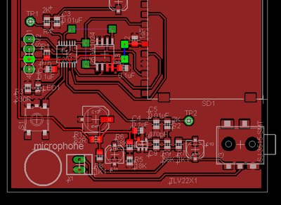
[Limpkin] begins his overview by mentioning that the schematic editors are comparable; the differences start to show themselves in the PCB layout tools. Here you can see that Altium always labels the pads so you know what net each of them belongs to. Cadence (whose PCB layout tool is called Allegro) will display the net if you hover over the pad with your mouse. Both have 3D rendering, with Altium’s looking a bit more pleasant but what real use is it anyway? Okay, we will admit we love a good photorealistic board rendering, but we digress. The most interesting differences show themselves once traces are all on the board and need to be rejiggered. Cadence will actually move traces on other layers automatically to avoid collision with a via that is late to the party, and Altium shows some strange behavior when dragging traces. [Limpkin] doesn’t register a final judgement, but the comparison alone is worth the read.