Control boards for 3D printers are a dime a dozen on the usual online marketplaces, and you usually get what you pay for. These boards can burn down your house thanks to a few terrible design choices. [Scott Rider] aka [Crow] took a look at the popular Melzi board, and what he found was horrifying. These boards overheat right at the connector for the heated bed, but the good news is these problems are easily fixed.
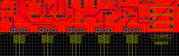
The Melzi board has a few problems with its PCB design. The first and most glaring issue is the use of thermals on the pads for the heated bed connector. In low-power applications, thermals — the method of not connecting the entire top or bottom layer to a hole or pad — are a great idea. It makes it easier to solder, because heat isn’t transmitted as easily to the entire copper layer. Unfortunately, this means heat isn’t transmitted as easily to the entire copper layer. In high-power applications, like a connection to a heated bed, these thermals can heat up enough to melt a plastic connector. Once that happens, it’s game over.
Other problems were found in the Melzi board, although you wouldn’t know it just by looking at the Eagle file of the PCB. [Scott]’s Chinesium Melzi board used 1-ounce copper, where 2-ounce copper would be more appropriate. The connector, too, should be rated above the design power loading.
[Scott] made a few tweaks to the board and also added a tiny DS1822Z temperature sensor to the high-current area of his version of a Melzi. Imagine that, 3D printer electronics with a temperature sensor. Slowly but surely, the state of 3D printer electronics is clawing its way to the present.
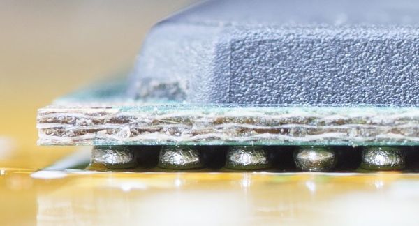
 The project [Andy] had in mind for these chips was a generic dev board, which meant breaking out the IO pins and connecting some SRAM, SDRAM, and Flash memory. The first issue with this project is escape routing all the balls. Xilinx published a handy application note that recommends specific design parameters for the traces of copper under the chip. Unfortunately, this was a six-layer board, and the design rules in the application note were for 5/5mil traces. [Andy]’s board house can’t do six-layer boards, and their design rules are for 6/6mil traces. To solve this problem, [Andy] just didn’t route the inner balls, and hoped the 5mil traces would work out.