A homemade seven-segment OLED display

Making OLED Displays In The Home Lab

Just a general observation: when your project’s BOM includes ytterbium metal, chances are pretty good that it’s something interesting. We’d say that making your own OLED displays at home definitely falls into that category.

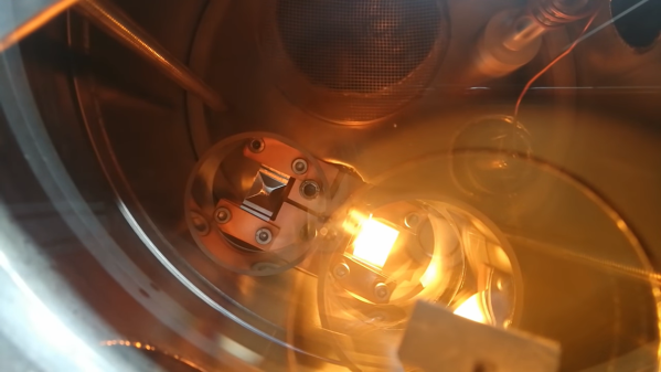
Of course, the making of organic light-emitting diodes requires more than just a rare-earth metal, not least of which is the experience in the field that [Jeroen Vleggaar] brings to this project. Having worked on OLEDs at Philips for years, [Jeroen] is well-positioned to tackle the complex process, involving things like physical vapor deposition and the organic chemistry of coordinated quinolones. And that’s not to mention the quantum physics of it all, which is nicely summarized in the first ten minutes or so of the video below. From there it’s all about making a couple of OLED displays using photolithography and the aforementioned PVD to build up a sandwich of Alq3, an electroluminescent organic compound, on a substrate of ITO (indium tin oxide) glass. We especially appreciate the use of a resin 3D printer to create the photoresist masks, as well as the details on the PVD process.

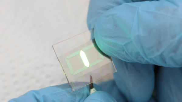
The displays themselves look fantastic — at least for a while. The organic segments begin to oxidize rapidly from pinholes in the material; a cleanroom would fix that, but this was just a demonstration, after all. And as a bonus, the blue-green glow of [Jeroen]’s displays reminds us strongly of the replica Apollo DSKY display that [Ben Krasnow] built a while back. Continue reading “Making OLED Displays In The Home Lab”

Thin Coatings Require An Impressive Collection Of Equipment And Know-How

Let’s be honest — not too many of us have a need to deposit nanometer-thick films onto substrates in a controlled manner. But if you do find yourself in such a situation, you could do worse than following [Jeroen Vleggaar]’s lead as he builds out a physical vapor deposition apparatus to do just that.

Thankfully, [Jeroen] has particular expertise in this area, and is willing to share it. PVD is used to apply an exceedingly thin layer of metal or organic material to a substrate — think lens coatings or mirror silvering, as well as semiconductor manufacturing. The method involves heating the coating material in a vacuum such that it vaporizes and accumulates on a substrate in a controlled fashion. Sounds simple, but the equipment and know-how needed to actually accomplish it are daunting. [Jeroen]’s shopping list included high-current power supplies to heat the coating material, turbomolecular pumps to evacuate the coating chamber, and instruments to monitor the conditions inside the chamber. Most of the chamber itself was homemade, a gutsy move for a novice TIG welder. Highlights from the build are in the video below, which also shows the PVD setup coating a glass disc with a thin layer of silver.

This build is chock full of nice details; we especially liked the technique of monitoring deposition progress by measuring the frequency change of an oscillator connected to a crystal inside the chamber as it accumulates costing material. We’re not sure where [Jeroen] is going with this, but we suspect it has something to do with some hints he dropped while talking about his experiments with optical logic gates. We’re looking forward to seeing if that’s true.

Continue reading “Thin Coatings Require An Impressive Collection Of Equipment And Know-How”