Back in the day where the microprocessor was our standard building block, we tended to concentrate on computation and processing of data and not so much on I/O. Simply put there were a lot of things we had to get working just so we could then read the state of an I/O port or a counter.
Nowadays the microcontroller has taken care of most of the system level needs with the luxury of built in RAM memory and the ability to upload our code. That leaves us able to concentrate on the major role of a microcontroller: to interpret something about the environment, make decisions, and often output the result to energize a motor, LED, or some other twiddly bits.
Often the usefulness of a small microcontroller project depends on being able to interpret external signals in the form of voltage or less often, current. For example the output of a photocell, or a temperature sensor may use an analog voltage to indicate brightness or the temperature. Enter the Analog to Digital Converter (ADC) with the ability to convert an external signal to a processor readable value.
ADC’s
Converting analog to a digital format involves tradeoffs: how often you need to be updated as to the signal (sample rate), how much you need to know (resolution), and the cost (how much you have in your pocket). High resolution and high speed tends have higher cost.
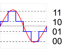
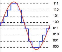
The act of converting an analog value to a digital representation is somewhat error prone, and the tradeoffs deal with just how much error we can tolerate. Looking at the two diagrams below we see a 3 bit digital representation of a sine wave. The area between the blue digital “steps” and the red line indicates an amount of distortion of the original signal. Using more steps, or digital values and bits, we can reduce the distortion and our digital copy gets closer to faithfully representing the true signal.
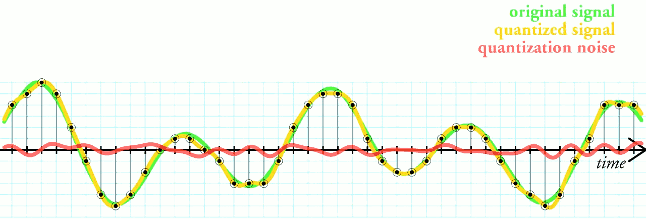
Also important is the sampling rate, or how often we convert the analog signal to its digital counterpart. Just as too few voltage “steps” (resolution) results in distortion, too few steps in time (sample rate) also results in distortion. In this diagram the distance between the green and yellow lines represents time-based distortion as shown in red.
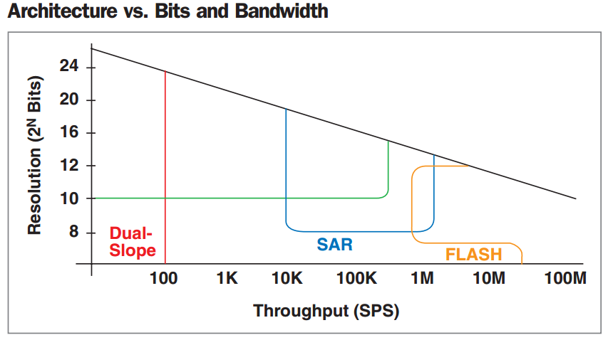
Types of ADC’s
Looking at the chart below we see four of the most common ADC technologies and their capabilities. I could probably spend an entire video post talking about Delta Sigma as it combined digital and analog processing, here I will concentrate the other three: Flash, Successive Approximation and Dual-Slope.
Flash Type Converter
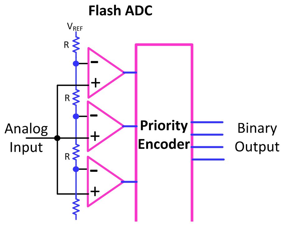 The Flash converter is the fastest, hence the name, but with some inherent limits to resolution and not without some cost involved. A flash converter is a collection of high speed comparators each with a slightly different voltage reference that they are comparing the signal to.
For 8 bits of resolution, a total of 256 comparators are needed along with the supporting number of semi-precision resistors. Likewise a 10 bit converter needs 1024 comparators and herein lies the reason why flash converters, as high speed as they are, are somewhat limited in resolution due to the problems with scaling as the number of bits increase.
Also shown is a discreet signal to binary encoder known as a priority encoder. This logic creates a binary value representing the highest comparator active (think of it as the opposite of a decoder such as those used to create 8 chip selects from 3 address lines).
Successive Approximation Register (SAR)
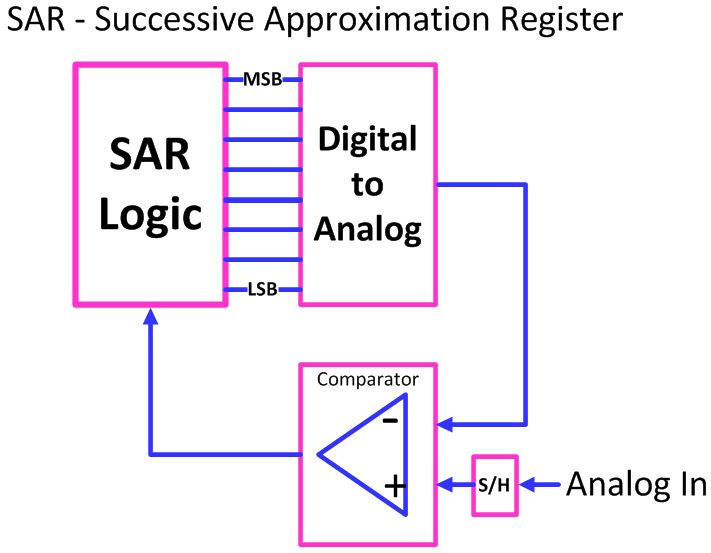 SAR utilizes a built-in Digital to Analog Converter (DAC), the opposite of an ADC, and compares the input signal to the output of the DAC and makes adjustments until it closely approximates the input signal.
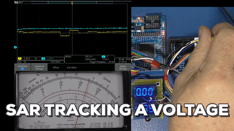
The SAR starts by first taking the MSB of the DAC value and setting it, representing 1/2 of full range, and then testing whether the input is greater or less than that value. The SAR then sets the bit if it was greater, and then tests the next bit representing 1/4 of the total. The SAR walks the bit on down testing for 1/8, 1/16, 1/32 on down to the LSB, all the while setting a bit for when the input was greater.
This series of approximations gets more accurate as more bits are tested, effectively hunting down the best approximation for the voltage it is testing against. I show some examples using a spreadsheet to represent an 8 bit SAR.


 First D7 is tested and if D7 is greater than the input (represented by red crosshatch) a zero is recorded, otherwise a 1 is stored and D6 is tested (while remembering the state of D7). The conversion uses one cycle for each bit, so the SAR conversion shown takes 8 cycles each time (vs. a single acquisition time for flash).
I walk through this in the video but if you want a chance to work through this hands-on you can download the SAR Calculation Spreadsheet.
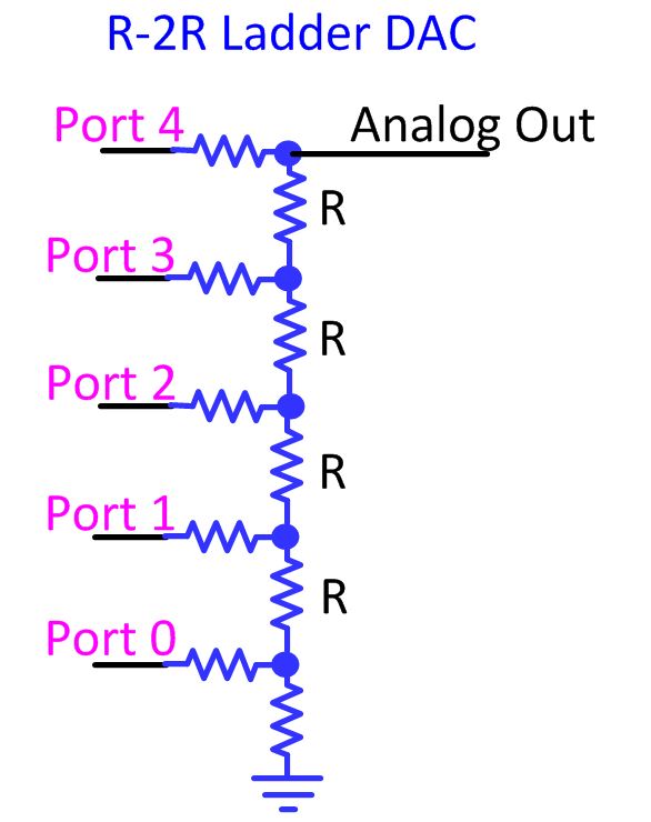
I have built an SAR system using an FPGA to provide the control logic, our R-2R Ladder that we built in the DDS video, and a simple comparator. Ever see a microcontroller with a 1-bit comparator and wonder why it’s there? Here is one reason; you can make an SAR with a handful or resistors on I/O ports and a 1-bit comparator.
Sample and Hold
As stated, an 8 bit SAR takes 8 cycles to complete an acquisition. During this time it is important that the voltage not change value as the series of approximations take place.
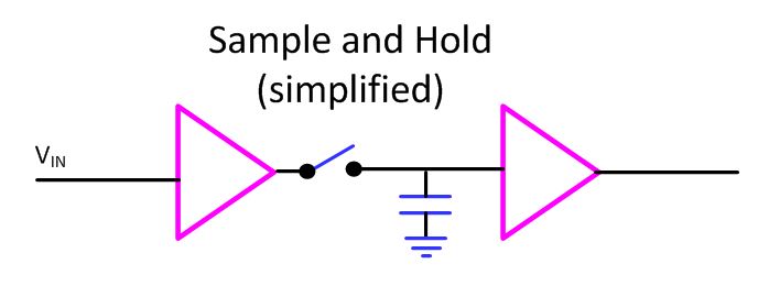
Enter the Sample and Hold (S/H) circuit. In its simplest form it captures the signal value in the form of a charge on a capacitor and then is isolated by a switch that disconnects the input. S/H circuits are available as integrated circuits that also do things like minimize the discharge of the voltage on the capacitor, known as droop, and to make sure that the switch affected the signal a minimal amount.
Dual Slope
Dual Slope conversion is named after the fact that it integrates the input signal for a known period of time, which results in an accumulated charge equal to the input signal, while providing some low pass filtering in the process. The charge is then integrated off by applying a known reference voltage in the opposite polarity and counting clock pulses until the signal returns to zero. Between each of these measurement cycles is an auto-zero phase which helps remove effects like drifting baseline.
Dual-Slope is used in instances where higher resolution is needed and conversion time isn’t as critical. As Dual-Slope can also be low power consumption it is often found in handheld devices like Volt-Ohm Meters or in the example I show at the end, precision digital weighing instrumentation.


The output of Dual-Slope is ultimately a string of clock pulses though they may be internally converted to a binary value such as in the case of the TC7109 IC I show above. In cases where output is a string of pulses that need to be counted, a microcontroller can count them using dedicated counting circuitry or counting overflows of an external divide down counter where each overflow represents a known quantity of pulses. A trick for using an external counter to do scaling and yet get the benefit of the full resolution is to then manually pulse the counter until the very last overflow is detected. The number of manual pulses it took is used to determine how many were left in the counter after the acquisition phase.
Putting it Together
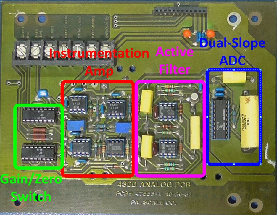
Below you can see a precision analog section I did back in 1982. Included in the design is a Dual-Slope ADC, an Instrumentation Amplifier with Zero and Gain correction (similar to Chopper-Stabilized or Zero-Drift amps) and active filters, all of which we have covered in Hackaday videos. The design is still viable however it is now possible to replace the instrumentation amplifier with a small dedicated chip and the dual-slope converters run faster with smaller capacitors, which takes some of the requirements off of the capacitor to not exhibit quite as low of leakage or dielectric absorption.
Conclusion
Understanding how an ADC works can be useful in understanding the results returned, or whether a different technology should ultimately be used. These days with SPI and I2C interfaces available on a wide array of ADC’s they can be connected to almost any processor architecture with minimal need to consider data bus architecture and timing.


Awesome info. I’ve got a project I’m working on with converting analog voltage to digital and I can never get a definite answer, so maybe the hive mind can help me here. I’m tapping a 12 volt auto signal (which generally reads 0v to ~14 volts) and converting the range into something a microcontroller can read. I’ve been working with Arduino, RPi (1B-rev2), and a Beaglebone Black. From what I’ve read, they are 3 to 5 volt logic boards. So, what are ways to handle 12 volts into the microcontroller without frying anything?
Agreed, good info, I’ve come across the SAR ADCs in pic32 and was wondering how they worked. Now I know, thanks :)
@CJ Rose
Either use a resistor voltage divider (http://www.raltron.com/cust/tools/voltage_divider.asp) or use an opamp if impedance is important (http://yano.wasteonline.net/electronics/opamp/index.php?mode=1). You can add a capacitor to filter out noise if necessary.
A simple voltage divider with a 10k resistor and a 1K resistor and you measure the voltage across the 1k will give you about 1.1v for a 12v input. You can calculate other values without knowing the math by using online calculators such as http://www.raltron.com/cust/tools/voltage_divider.asp I would probably add a diode (anode) from the junction of the resistors to the VCC of the microcontroller (cathode) so that the voltage never ever is greater than the supply for whatever reason. You may also want to add a 35V or 50V MLC cap of .1 – 1uf as a guess to smooth the voltage out. Just be aware that there are big spikes on automotive power lines due to big inductors such as the starter. You can send a schematic snippet to me at bilherd at hackaday.com if you would like me to take a glance at what you come up with. Bil
Voltage divider: two resistors in series. Easy. The voltage at the node between them will be some fraction of the voltage at the top. An example would be a 1K Ohm resistor on top, and a 300 Ohm resistor on the bottom. This will take an input voltage of 14V at the top and drop it down to about 3.2V. In your micro controller, just multiply that value by 4.333.. and it will tell you the original voltage.
As always, there are caveats. These two resistors will add to 1,300 Ohms, and you will be applying 14V across their combined resistance. This means, I = V/R = 14V / 1,300 = 10.8mA will essentially be wasted as heat (150mW) by this circuit all the time. You could just as easily use a 10K and a 3K resistor to get the same divider ratio, and 1/10th the current, but doing this also makes the signal less-robust (higher source-impedance). So, if you did this, an op amp buffer would need to be employed between the divider output and the analog input, because the measurement pin on your microcontroller will certainly load the signal down and alter the readings.
Adding some capacitance across the bottom resistor will effectively filter (averaging) the signal to make it smoother and you’ll get nicer looking data. If you go too far, the response will be very slow.
TL;DR All you need is two resistors to have something functional for what you want to accomplish.
Engineering is always an exercise in compromise.
Thats a good point in in that the divider will look like a load on the battery always and forever. In the old days when you turned your key off everything was off, not as much these days. (I had to pull an alarm from one of my cars as it killed the battery in a couple of weeks if parked.
Using as high of impedance of resistor divider (or other cool tricks that are more complicated) as practical for the ADC would be best
Best would be to use alogic level MOSFET to enable or disable the resistor divider.
Resistor divider should be sized to match the required input resistance specification limit of your micro, that would probably be under electrical pararmeters in the datasheet.
The filter cap is important as the voltage divider has a high impedance. As the sample and hold (essentially a small capacitor) inside the ADC goes into sample mode, it’ll require some current for charging up. Without the filter cap providing the charge (low impedance), this charging current will cause a voltage drop from the divider and affect the reading.
For high frequency signals, the cap can act as low pass filter. You can calculate the proper value to make an anti-aliasing filter to be below 1/2 of the sampling frequency.
Also, don’t forget that ATMegas claim to work best with about 10KOhm impedance.
“You can calculate the proper value to make an anti-aliasing filter to be below 1/2 of the sampling frequency.”
Not correct, and a common mistake which gets very difficult to recover from.
What you really need is an antialiasing filter that *rolls off into its stop-band* below half the sample rate.
Just how far it has rolled off at that point is often what determines the ultimate accuracy of the convertor. (Assuming you do lots of averaging).
If you design your antialiasing filter to just start to roll off at half the sample rate, then you could induce an error voltage up to half the full scale of the input, as the attenuation will be only 50% at the design point of the filter.
This is easy to show: just high-pass filter a square wave function gen set to full scale voltage amplitude, and play with the precise frequency of it around the convertor’s sample rate, and you will see that you can produce not just an apparently steady DC offset, but just about any arbitrary signal by modulating the phase (playing with the frequency knob on the function gen).
In general, if you care about reconstructing events from the data, then you want an anti-aliasing filter with maximal group delay flatness in its pass band. So either single pole, or double pole Bessel (not Butterworth!). This means that it’s step response settles quickly without oscillation. The time it takes to do so (the width of the impulse response waveform, which is just the d/dt of the step response) ) is your ” time precision”.
Combining the two above details, you will end up needing to be sampling multiple points across the impulse response anyway, and it turns out that simple moving averaging filtering is all you need on the digital side afterwards.
You end up with a smoothly varying data stream, which will faithfully reproduce the input voltage without adding extra oscillations and “noise” such as that from aliased signals.
The last trick is: if you are going to need the d/dt of a voltage signal, then *DON’T* decimate!
Just accept that any step will take multiple samples, and that your “time precision” is many times less than your sample period: by the number of samples a step response takes to settle, of course. This will mean your ADC will necessarily be “rate limited”, ie, unable to follow dv/dt signals any faster than its best step response, but in return for all this hassle, things like fast PID loop control will tend to be much more robust against electrical noise such as what welders and high power inverters tend to emit.
(Mostly this is because if you just set your AAF 3db point = 1/2 fs, you can practically *guarentee* that there will be high order harmonics of 50/60Hz which are in that “barely attenuated” gap about 1/2fs, and which aren’t quite synchronous to your 10.000000 MHz clock crystal (or whatever decimal factor of a MHz it uses). Your sampling will shift all of these harmonics (even possibly those which your filter might not catch at all, for instance due to the caps going inductively resonant in the VHF to UHF band) so they lie right on top of each other, which will mean the error caused by them can fortuitously add… creating an error signal larger than expected, which comes and goes more or less at random, because the mains power frequency isn’t exactly synchronous to the sample clock, just almost.
I rant on this here so much because this one pitfall is so incredibly common.
Your ADC is only as accurate as the rejection of its antialiasing filter for all bands from 1/2 fs, all the way up to the natural -3db input bandwidth of the ADC convertor IC itself!
And your “time accuracy” to localise events is only as narrow as the convertor’s impulse response after all applicable filtering.
(If it overshoots by 20% or so like a Butterworth filter will, then your convertor’s “precision” nearby any disturbance is only good to +/- 20% as well! Because, how do you know there isn’t another actual event pulse hidden in there? And given that “noise” look like a background of little, random impulses, how do you know a pulse you see isn’t just resonance of the AAF filter excited by a couple of fortuitously-timed “noise” glitches?)
Yes in the video I describe it better. Being above the Nyquist is the bare minimum to determine the bare minimum about the signal (without even really describing what Nyquist really is) . There is also a limited time in which to hit the topics, so when I say “better’ in the video I mean something like 3 sentences. All of what you said appeared to be true at a first glance and not a lick of it would have made it through the editing process.
Fair enough – it’s a good stuff, short and sweet!
I must confess when I first posted I hadn’t actually sat down to watch the video at that point. I wasn’t criticizing you, more knee-jerk reacting, sorry!
This is REALLY good. You should write a book (maybe just some tutorials) on DSP, or at least be involved-in the writing of one. Excellent explanation.
Thank you.
If you are measuring the 0->14V across the battery terminal and you do not want to be slowly discharging the battery with two resistors across the terminals. You might also add a normally off relay into to your circuit with a Flyback diode across the relay to protect your circuit from back EMF when the relay is powered off. For some reason digital circuits do not like -400 volts being applied to them for 20 microseconds. ( https://www.youtube.com/watch?v=43HFng0CVKg ). So you would use a GPIO pin to engage the relay which would put your voltage divider across the battery terminals prior to measurement. This would make sense if you were only measuring the voltage once an hour/day. But if you were measuring every second it would probably just adding another point of failure.
Alternatively, a MOSFET with a pull-down resistor to gate can be used instead of a relay.
Thanks guys! I’ll have to revive my hastily soldered together VD’s and experiment. I’m measuring voltage through the wiring harness connecting to the gauges for sensors (such as coolant temp and fuel level). Most of these are to be consistently measured and digitally interpreted. The only one that’s really really giving me issues is how to convert the constant 12 volt signal from the RPM wire, which is a square wave, to a format I can use digitally.
Add a resistor divider for it, then measure the intervals – like, for how long it’s high and for how long it’s low, think it should work with that =)
First:
Automotive applications should comply with load dump conditions ( your 14v max is actually 60v or 100v or 200v depending on the type of vehicle.)
Second:
The BBB ‘s ADC is 1.8Vmax, not 3.3V.
Third:
I did not see ENOB or supersampling mentioned here.
Fourth:
How much accuracy does your measurment need? +/-1v? +/-1mv?
To get an idea of what’s going on open up the datasheet for an AFE and look at the block diagram or application diagram.
The normal Arduino environment uses the 5 Volt Vcc to the ATmega328p-pu as the analog reference for the ADC and that is a problem because the the 5 volts is not an accurate reference.
This problem can be solved but remember you have to divide your test voltage down so that it is less than the reference at all times.
Solution 1) Use the internal reference (1.2 Volts from memory) to calculate any inaccuracy of the 5 Volts and use math to “fix” the normal analog in.
Solution 2) Divide your signal down to below the reference and use the internal 1.2 Volts as the reference.
Solution 3) Make a hardware external reference that is more accurate.
The config or the way the ATmega uses it’s reference can be changed with snippets of code that directly set the resisters. These snippets of code are out there on forums / libraries etc.
Excellent visualization of SAR searches and dual slope integration.
Thanks. I was somewhat surprised the spreadsheet example was somewhat usable.
Most of the projects I build use an Arduino as a controller and run on batteries. I check battery voltage on startup to make sure the battery voltage is adequate to run the system. I use a simple voltage divider to measure the voltage and use this code for all the projects. Since I usually only check voltage on startup, I use floats and don’t worry about the time it takes.
If you are doing measurements throughout the application and want faster readings you can select values that give an integer result to the R1+R2/R1 formula and just use that value instead of computing it every time.
// used for battery monitor
float SupplyVoltage = 0; // Power supply voltage
#define vin_BAT A1
// voltage divider values
// select values depending on allowable current consumption and maximum voltage to measure
#define R1 (100) // from GND to vin_BAT, express in 100R (100 = 10000 Ohm)
#define R2 (330) // from + power supply to vin_BAT, express in 100R (33 = 33000 Ohm)
SupplyVoltage = analogRead(vin_BAT); // Read power supply voltage
SupplyVoltage = map(SupplyVoltage, 0, 1023, 0, (500 * (float R2 + float R1) / float R1)); // compute battery voltage using voltage divider values
//SupplyVoltage = SupplyVoltage + . 70; // ADD if using a reverse voltage diode in battery circuit
Why not measure against the internal 1.1 reference? No io needed
I really like Bil’s stuff. He obviously knows what he’s doing and he does try to present it in an understandable and factual manner.
That said, I do have some gripes about this video. I think you’d profit from putting more work into writing the script about what you want to say. I’ve done hobby-level electronics for years, with sporadic research sessions trying to find out how stuff works and replicate it, so I personally didn’t have problems understanding it. However, I know that some aspects of this video are just plain confusing, such as the interspersed discussions about different kinds of errors of ADC, quantization errors and sampling errors. A bit more planning there could have made this much clearer. I would have preferred the discussion about general problems of ADC to be in its own segment or video after all the different ADC types have been discussed. I know that it can be hard to focus on just one topic; where analog meets digital, so many things are equally important that one might be tempted to try to explain everything at the same time. Don’t do that! It’s confusing. Explain one thing, then explain the next thing, even if they are both important to know to fully grasp the concepts. I tend to prefer non-confusing explanations that allow me to get the gist over confusing explanations that explain everything.
The content surely is there, it’s just the presentation that could be improved quite a lot by rather minor tweaks. I really like the experiments on the bench, they’re just great.
Really looking forward to the sigma-delta video.
Yeah I had one of those moments of wondering if I should lay some ground work when I hadn’t planned on talking about quantization at all. What I have to be careful of is suddenly I am 20 minutes into just talking (lecturing) and that doesn’t sound very interesting to me. I admit I treat some things as “know this exists so you can research more” before I dash off to the next topic in order to keep things moving and try and hit a 12 minute video.
Thanks for the feedback!
Seems like some real smart people are gathering here, so I shoot my question too.
I co-designed a circuit couple of year ago, it was a 5V microcontroller in the middle (pic at the time),
and all input was opto-coupled, and all output was relay output.
We should have added an analogue input, which would measure 0-10V (or 4-20mA),
in a way, that accidental wrong wiring do not fry the whole board.
By wrong wiring, I mean someone accidentally put 220V for one of the terminal (happened
multiple times, fried some optocouplers, but nothing serious).
But I got completely stuck at the problem, how to protect an input while reading 0-10V still possible.
The best we could come up, was some external AD converter chip, which communicates through
optodiodes. But they would need yet another power supply,
the whole thing started to look too complicated, and expensive.
I would love to read up in this domain, so any pointer or book recommendation is really interesting to me.
(if it a blogpost then even better!)
Hope it is not too offtopic or nagging…
How about a resistive voltage divider with equal resistor values?
Dividing down the 10V max to 5V max?
The value of the input resistor determines the input impedance.
Or, you could use an op-amp, with the feedback resistors sized to produce a 0.5V per volt gain. Input 10V, and it outputs 5V.
For input protection in the 4-20 mA industrial environment, I’ve used Zener diodes.
Yeah isolation in 4-20 is a highly desired attribute. Used to be you could get some modules that provided the conversion and isolation but they had some cost to them. I have used optocouplers and the isolation of a separate transformer tap for a separate power supply and if I were designing for industry I would start with that concept and then see what modern tech allows. Keeping leakage current out of your signal loop is also desired.
For some quick and symmetrical or asymmetrical ESD and over-voltage protection I usually look at silicon made specifically for the task such as Transzorb. Fast Zener’ish (avalanche) devices made for heavier lifting. In industry big welders can cause a 1mhz, 1kv voltage and they were fast enough to catch it and hefty enough to keep working.
This is a pretty tough problem actually. Simplest solution that I’ve run across is to use an SPI ADC and one of Analog Devices iCoupler chips with 4-channels and a DC-DC converter. Otherwise if a KHz or less of bandwidth is acceptable, you can operate an opto-coupler in linear mode. Plugging “isolated amplifier” into Google image search shoul up quite a few results.
Optocouplers are available just like transistors…. Dual parts matched in the same due process with very little drift between them.
Think of how a current mirror works. It requires matched transistors to work really well over full temperature range.
Now think of a current mirror that uses matched pair optos…
You’re welcome…
Most modern micro-controllers have very high input impedance now and that’s why they can do capacitive touch.
This means you can use high value / high voltage resistors as the divider. Just make sure that you have wide haps to the voltage can’t arc over. You will need reverse biased diodes to both of the micro-controllers power rails. This method however assumes the ground connection is safe.
Alternatives –
As above but us the external voltage to run a voltage to frequency converter and have an optocouple between there and the micro.
As above but with high value resistors for both the test voltage and the test ground and feed them into a instrumentation amp (op amps in differential mode).
“Below you can see a precision analog section I did back in 1982.”
Bil, was this back when you worked for Pennsylvania Scale? (I think I remember reading about that in the Bagnall book.)
Looks like it, check the board label below (PA Scale).
Yes. Terry Fisher (PCB Guru) and Hedley Davis (Amiga, X-Box) came from there as well.
Please tell me that there is a ground plane beneath those parts…
$10 Chinese counterfeits of REX-C100 Temperature Controller are build super cheap using lowers of the cheapest chinese (stc/megawin) 8051 clone microcontroller combined with 74HC74 dual flip flops and an opamp (LF353/TL072/TL082), plus cd4051 for multiple thermocouple inputs = Dual-Slope converter = precision adc for <$1
Its amazing what works “good enough”.
TL072,the replacement for TL082’s usually had an input whose common mode range did not include ground. That means their output would slam to whatever rail it felt like if the input went to 0Vdc in a singled-ended (powered by DC to ground, no negative power input) application.
You don’t really know the value of rail-to-rail inputs and outputs till you’ve been burned by one of these older parts.
The superimposed quantized noise graph got me thinking: is it feasible to add a stage where the circuit compares the original waveform to a reconstructed sample of the quantized waveform using an analog comparator, then uses an op-amp on the quantized noise by itself (comparator result) and runs the noise back through the DAC to fill in the reconstructed sample?
oh whoops guess i should’ve read the whole article and gotten to the SAR part first before commenting :)
Wait until I talk about Delta-Sigma ADCs!
“A True Understanding”? Pfffft… Where are the ADC subjects of noise, dithering, interleaving, on-and-on? Nowhere – as usual. This is just another “Half-Way Done Herd” tutorial. A real disservice to the readers.
I don’t pick the title, but yes this is no more than a brief dashing between a couple of subjects in the hopes that someone may get a visualization of something that sticks with them and encourages more research if interested. The whole time I am discussing the topic the issues of the thoughts of linearity errors and error accumulation flit through but to do a lecture would require the time it takes to do a lecture. The thought that this is half-way done is somewhat understated, it would take many many brief videos to really cover the topic, not two.
A *Single*-Slope ADC is easy to understand: Use a resistor, capacitor, and op-amp to form an integrator. Then measure the time it takes for the unknown voltage to charge the capacitor to a known referenece voltage. It’s simple, but the disadvantage is that the result will be only as good as the tolerance of the R and C used.
The advantage of the *Dual*-Slope ADC (that the article failed to mention) is that it uses the *same* components for the “integrate” cycle of the unknown voltage, and compares that against the “de-integrate” cycle to the known reference voltage (hence the “dual” slope). Simply stated: integrate the *unknown* voltage for a *fixed* period of time; then de-integrate to a *known* voltage which takes a *variable* period of time.
When you do the math, the Rs and Cs cancel out (so the dual-slope design is immune to part tolerance). In the end you are comparing the number of clock used to integrate to the number of clocks used to de-integrate. If the clock is stable (and it is) you can get very high resolutions, in excess of 24-bits.
A look at the 710x-series datasheet, shows the internal logic which is little more than a binary counter and control logic and analog switches. A judicious choice of 1000 clocks for the “integrate” cycle, means that you can eliminate the need for math during the *de-integrate* cycle, and display the count directly as the result.
The post is a heavily abbreviated version of the video where I talk about that exact point of the reference phase and also the auto-zero phase. I also show that the slope of the reference phase is consistent and that the integration of the input signal provides some filtering. Additional text was also cut about how to count large number pf pulses yet with high resolution as the post gets unwieldy pretty quickly. (so that you could have 1000 pulses representing 1,000,000 pulses of resolution using a counter that is then queried for remainder)
For those like me who didn’t or haven’t yet watched the video …
Single slope (non-iterated) gives very poor accuracy in analog to digital conversion because the charge and discharge curves of a capacitor are non-linear. They are an exponent of time and the inverse of same for discharge.
This doesn’t really matter than much if the purpose of the overall system is go both ways. For example if you need to convert an analog signal to a bit stream and then back to an analog signal then the overall accuracy is much better if the same Capacitor/Resistor configuration is used for both: conversion to digital and also conversion back to analog. The error at one end tends to cancel the error at the other end. This does however have a different effect on quantizing error.
There are two ways to fix this error to some degree.
1) If, like the example above, you are converting back to analog then you can use dual slope and the exponential charge curve of the capacitor is somewhat canceled by the inverse exponential discharge curve making the overall system a little more linear.
2) … and there is much more to this …
An op-amp can be configured like a little analog computer that yields the correct result of a mathematical function or equation all the time unlike a micro-controller that is correct so many times a second.
One of these functions is an integrator and it can take a square wave from a micro-controller and turn it into a perfect saw wave that is perfectly linear.
With this method the non-linearity of a capacitors charge/discharge curve is completely eliminated and the converted digital representation of the analog signal will be far more accurate.
I thought I would mention this because op-amps and signal per-conditioning are by far underutilized in modern designs.
Some are put of by the mention of maths or the mystery of op-amps, in reality it’s all been done before so a bit of google fu will find the exact design you need without having to do any complex calculations.
Also – good to see another article from [Bil Herd], hopefully I will get time for the Video on the weekend.
When I see an RC slope turned into a straight integration because of the cap being in the feedback loop, part of me thinks “magic”. An Opamp feedback loop has mystical powers: it can make a diode”perfect”, and a slope “straight”. (minus the errors due to bias current, etc etc etc)
So could you use the flash method as a module to replace a comparator in a SAR? I guess you’d need variable resistors for that to work. So instead of a binary comparator per cycle, you could have 8bit comparator and settle more quickly on the input voltage (or same time and higher resolution).
Better, you can ‘unroll the loop’ and pipeline a series of such modules. This then lets you perform a series of fairly high bit width conversions very quickly, without having to have stupid numbers of comparators.
Each sample gets converted over a series of cycles, so there’s some latency, but you get a new sample completing conversion every cycle, because of the pipe lining.
Pretty much all high bandwidth, high precision converters work this way. You can have ~14 bits effective at >100 MHz this way.
This isn’t as technical as some of these posts, but here goes…
For a quick (or perhaps I should say slow) and dirty ADC, I am using an atTiny 4313. The PWM (Through an/a LP filter) provides the compare voltage that would usually come from an R/2 ladder. By ramping up and breaking out at the trigger voltage, then ramping down and breaking out again, I get two values that I add together (so it’s like an average, except I don’t divide them by two). Since the regulator runs around 5.12v it’s just 100x(sum of numbers). Three parts. One resister to protect the chip from a “too large” voltage. One for the LowPass filter, and a cap for same. You need a couple of milliseconds for the PWM to register fully on the LP filter before you check the comparator output..If you use SA it would take more time to settle I think, but you’d only need 8 iterations, so it would be faster overall.
Comments?
Oops. it’s (sum of numbers) / 100=voltage
> The area between the blue digital “steps” and the red line indicates an amount of distortion of the original signal.
Nope. https://www.youtube.com/watch?v=cIQ9IXSUzuM
That is so counter intuitive, but you can’t refute the measurements. Amazing!
I don’t fully agree with what he says about quantising *noise*. His demonstration uses a sine wave that will yield a perfect and predictably distributed noise that relates to the quantisation *error*. These points are a simple mathematical calculation on the difference between the input frequency and the sample rate and of course the sample depth (+ or minus half LSB).
Should he have simply spoken through the digitally link the he would have heard that the characteristics of the *noise* change with the input speech.
This is because of how the *not mentioned* DAC output filter works and the same explains the missing harmonics on the square wave.
A simple confusion between quantising noise and quanising error. It is only quantising noise after it has been modified by the output filter, before that it is quantising error.
Just to clarify. Noise in this case is referring to the human perception of noise. With a sine wave input the error will translate to a distortion that a human would not describe as noise. However, had he uses a complex input like simple speech then *noise* as a human perceives it would have been obvious.
Quantising noise not = quantising error
In the video I qualify that I meant distortion. Distortion is often then perceived as noise. Sometimes I accidentally jump to what something may mean to the viewer so that they can try and relate to what I am saying. Sometimes I also see error sometimes as also the injection of a a noise source also as an unasked for signal with it’s own attributes (such as being filterable).
But yes, I misspoke… it should be distortion.
Sorry [Bil Herd], I meant the video linked above by [Monty Montgomery]
I *still* haven’t had the time for your lol, after today’s email !
I have this weird wave file. It sounds so different when you re-sample it down to 22050. Can you hear the difference, and explain it?
https://drive.google.com/open?id=0BxjV7AG0dyW8OWhGclRyQWhtSHc
It’s only 11 seconds long.
If you mean the underlying sound, it sounds like a “fuzz pedal” to me which is an overdriving distortion technique that creates some interesting artifacts. Sampling may then affect the artifacts in interesting ways also.
No. The Fuzz was intentional. You really have tore-sample it to hear what I mean. B-)
This one should be re-sampled to 16000. It’s more apropos. As the principal involved relates to the lyrics.
https://drive.google.com/open?id=0BxjV7AG0dyW8QTBqUmhkcEtXZ0E
Have fun.
I can’t believe that nobody here is curious or smart enough to solve these puzzles.
Come on people, your reputations are at stake here.
Thank you for the Dual Slope explanation!
Hi,
I read a lot of helpful suggestion to convert 12V down to 3.3-5V to match with ADC channel on the Aduino board.
And i understand why. However, i ran into an accident by supplying 5V to ADC channel of DSPIC33EP512MU814(VDD specification at 3.3V). I am confused and wondering how come my accident did not fry my MCU. I always assume supply the voltage higher than the VDD will fry the MCU. Is my assumption correct?
Thanks for your help.
Minh