The fact that modern-day x86 processors still pretty much support the same operating systems and software as their ancestors did is quite a feat. Much of this effort had already been accomplished with the release of the 80386 (later 386) CPU in 1985, which was not only the first 32-bit x86 CPU, but was also backwards compatible with 8- and 16-bit software dating back to the 1970s. Making this work transparently was anything but straightforward, as [Ken Shirriff]’s recent analysis of the 80386’s main register file shows.
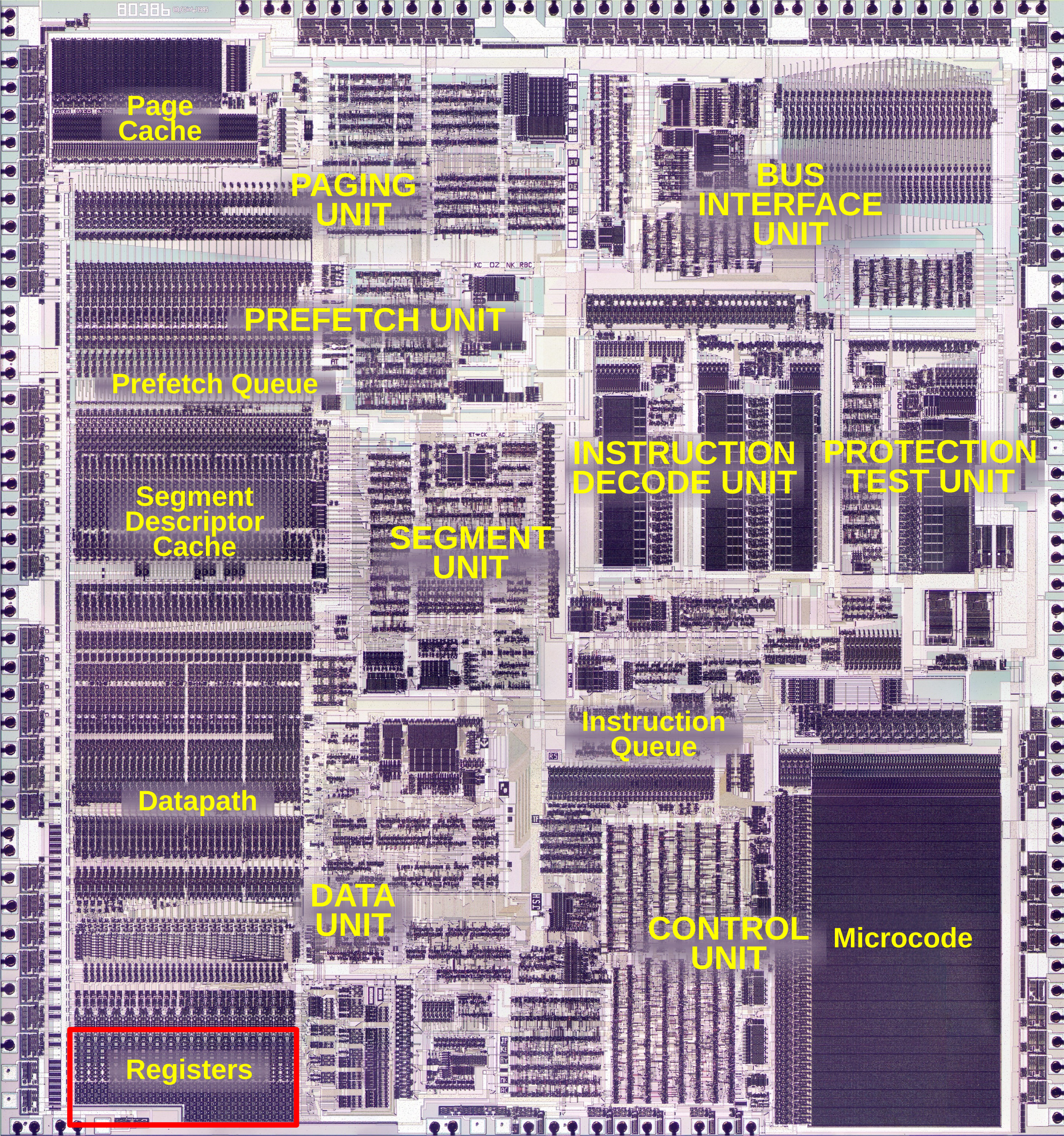
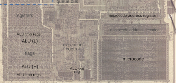
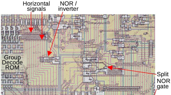
Using die shots of the 386’s registers and surrounding silicon, it’s possible to piece together how backwards compatibility was implemented. The storage cells of the registers are implemented using static memory (SRAM) as is typical, with much of the register file triple-ported (two read, one write).
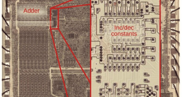
Most interestingly is the presence of different circuits (6) to support accessing the register file for 8-, 16- or 32-bit writes and reads. The ‘shuffle’ network as [Ken] calls it is responsible for handling these distinct writes and reads, which also leads to the finding that the bottom 16 bits in the registers are actually interleaved to make this process work smoother.
Fortunately for Intel (and AMD) engineers, this feat wouldn’t have to be repeated again with the arrival of AMD64 and x86_64 many years later, when the 386’s mere 275,000 transistors on a 1 µm process would already be ancient history.
Want to dive even deeper in to the 386? This isn’t the first time [Ken] has looked at the iconic chip.