Programming Tetris By First Building A Logic Gate, Then A Computer, Then…

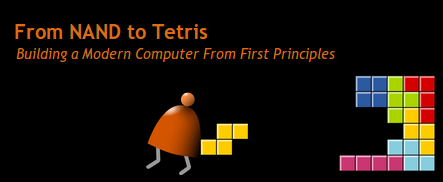
Hone your fundamental understanding of computer systems by completing this online course called NAND to Tetris. The idea is to develop each fundamental unit that goes into making computer programs a reality. This starts with logic gates, which are put together into modules that eventually become a functioning computer. From there you need an operating system,  a compiler, and eventually you’ll be playing a game of Tetris which you programmed yourself.

It’s certainly not an easy journey, but if you have a computer at your disposal you should be able to make it all the way through the course. There’s a software suite which includes a hardware simulator so that the computer you’re building can be assembled using HDL instead physical components.

The concept is discussed in this TED talk given by [Shimon Schocken]. It is also embedded after the break and in addition to the NAND to Tetris project he shows off some self learning software on the iPad. To us it seems very much like the learning software [Neal Stephenson] envisions in the Young Lady’s Illustrated Primer from his Diamond Age novel.

Continue reading “Programming Tetris By First Building A Logic Gate, Then A Computer, Then…”

Reading Bare NAND Flash Chips With A Microcontroller

NAND flash, the same memory chips found in everything from USB thumb drives to very expensive solid state disk drives, are increasingly common. As they (partially) serve as the storage for cellphones, Wiis, routers and just about every piece of consumer electronic devices, you’re probably surrounded by dozens of NAND chips at any one time.

[Sprite_tm], hacker extraordinaire, put up a build a few years ago where he was able to read the contents of NAND Flash chips using a PC parallel port. It’s getting rather hard to find a parallel port on a PC anymore, so he updated his build to read Flash chips off of a USB port.

There are two main components of [Sprite_tm]’s build. First, to read the Flash chip, he needed a way to break out the pins on the very tiny TSOP48 package. [Sprite] found a neat little socket for these chips on eBay for about 10 Euros.

Communicating with the Flash chip via USB was a little harder. [Sprite] knew he needed USB 2.0, but not many microcontrollers have that implemented. Luckily, the FTDI FT2232H has USB 2.0, along with the very nice feature of being able to read data and address pins directly from the Flash chip. After a bit of soldering, [Sprite_tm] was left with the device seen above.

[Sprite_tm] found a nice library to bitbang the pins on the FTDI chip and request one page of memory from the Flash chip at a time. The device works as advertised, but it’s still a bit slow at 250 kBps. [Sprite] figures he can increase the speed of reading a Flash chip by requesting multiple pages at a time, but it’s still orders of magnitude faster than the old parallel port solution.

There’s a good bit of software [Sprite] posted to help him (and possibly others) read bare NAND flash chips via USB. This means if you have a broken USB Flash drive or SD card, it’s possible to desolder the chip and read it with your own controller. Interpreting the blocks of data recovered from a Flash drive as a file system is another story, but it’s still a fairly remarkable build.

OLinuXino Booting Android

We can’t say the name rolls off the tongue, but it is beginning to look like the OlinuXino is going to happen. Here you can see the prototype hardware booting Android. If this is the first time you’re seeing the hardware you can think of it in the same category as the Raspberry Pi. It’s a butt-kicking ARM platform that comes as a bare-board with which you can do what you please.

Olimex Ltd. put together the offering, which seems to be part of the name mash-up (Olimex + Linux + Arduino?). The board hosts an ARM Cortex-A8 processor which runs at 1 GHz. There’s a half a gigabyte of ram, four USB and one USB-OTG ports, and a big array of breakout pins. One eyebrow-raising choice was not to include an HDMI connector. Instead the board offers VGA and Audio outputs. There is a pin header meant for an LCD screen, as seen in the image above, so it could be that the intention here is for smaller or more portable applications. But like we said, the form factor really lets you do what you want.

Possibly the best part is the price. The target for the top-of-the-line board is 55 Euros (about $68) and that comes with WiFi and 4 GB of NAND storage on the board. There’s a bunch of posts on the project, including a look at the PCB routing work. This link to the A13 tag will give you the widest overview of the work so far.

[Thanks Acce]

Computing With The Command Line

Here’s something we thought we would never see: computing with just pipes, /dev/zero, and /dev/null.

As a thought experiment, [Linus] imagined a null byte represented an electron. /dev/zero would have an infinite supply of electrons and /dev/null would make a wonderful positive power supply. With a very short program (named mosfet.c), [Linus] can use Linux pipes to control the flow of electrons between /zero and /null. [Linus] used mosfet.c with a very short shell script to create a NAND gate. From there all bets were off. He ended up creating a D flip-flop4-bit adder and a counter.

From a bit of cursory research, Linux has a maximum pipe capacity of 1,048,576 bytes and the maximum number of PIDs is 4,194,304 (correct us if we’re wrong). [Linus]  can theoretically build some of the classic CPUs of the 70s and 80s with his pipe logic. An Intel 486 is just out of reach, though. If you give someone a NAND or a NOR they’ll eventually build a computer; we thought we’d never see this, though.

Most Useless Machine Upgrade — Now With A Button!

There’s a soft spot in our hearts for pointless projects, as long as they’re well executed. [Bertho] really hit the mark with his take on the most useless machine. We’ve seen several renditions of this concept, most of them hinging on a box that will turn a mechanical switch off whenever you turn it on. But this take uses a push button to activate a switch flipping mechanism on another part of the machine.

You can see the drive gears in the image above. The final gear has a small bar which flips a switch to one side or the other. The circuit does this without the need of a microcontroller. A 7400 series NAND gate chip, some passive components, and two mechanical relays are all it takes. At each push of the button, the logic chip trips one of the relays to trigger the appropriate motor direction based on the current state of that switch. You can press the button during movement, but all that will do is delay the inevitable flip of the switch.

Extending The Battery Life Of LED Dominoes

[Fede.tft] wrote in to tell us about some work he’s been doing to save battery life for LED dominoes. He originally got the idea after reading this post about the electronic gaming pieces. That project was aimed at the 555 timer contest and therefore, used a 555 timer. [Fede.tft] calculates the battery life for the CR2302 battery in the 555 circuit at no more than about 80 days. That’s if you never use them and the LEDs are never illuminated. It makes sense to remove the batteries from the device when not in use, but a redesign to increase efficiency is definitely worth the effort.

This rendition does away with the 555 chip in favor of a CMOS chip. By building a circuit around four NAND gates of a CD4011 chip, the standby lifetime of the battery is calculated to increase to about 4.5 years. Not bad! Add to this the fact that replacing the 555 timer didn’t increase the component count, the price for the chip is similar to the 555, and you didn’t need to resort to a microcontroller. Yep, we like it.

Hardware-based Security Keypad Keeps It Simple

hardware_keypad_lock

Instructables user [trumpkin] recently built an all-hardware based keypad lock for a contest he was entering, and we thought it was pretty neat. The lock uses mostly NAND gates and 555 timers to get the job done, which makes it a nice alternative to similar software-based projects we have seen in the past.

The lock has 6 keys on the keypad, which is connected to the main logic board. The keycode is set using a series of headers at the bottom of the board, and you get 10 chances to enter the proper code before the board locks up completely. If this occurs, a “manual” reset via a button built into the main board is required before any more attempts can be made.

As you can see in the video below, the lock works quite well, but suffers from one shortcoming. Any permutation of the key code can be used to deactivate the lock, which is something [trumpkin] says he would like to improve in the future.

If you are looking for some more security-related reading, be sure to check out these other hacks we have featured in the past.

Continue reading “Hardware-based Security Keypad Keeps It Simple”