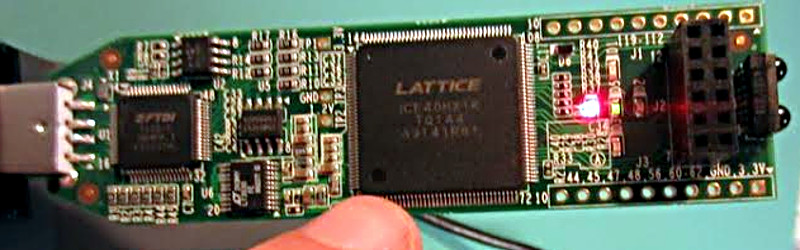
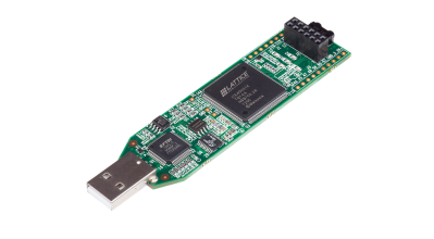
Over the last year we’ve had several posts about the Lattice Semiconductor iCEstick which is shown below. The board looks like an overgrown USB stick with no case, but it is really an FPGA development board. The specs are modest and there is a limited amount of I/O, but the price (about $22, depending on where you shop) is right. I’ve wanted to do a Verilog walk through video series for awhile, and decided this would be the right target platform. You can experiment with a real FPGA without breaking the bank.
In reality, you can learn a lot about FPGAs without ever using real hardware. As you’ll see, a lot of FPGA development occurs with simulated FPGAs that run on your PC. But if you are like me, blinking a virtual LED just isn’t as exciting as making a real one glow. However, for the first two examples I cover you don’t need any hardware beyond your computer. If you want to get ready, you can order an iCEstick and maybe it’ll arrive before Part III of this series if published.
I’m not going to directly try to teach Verilog. If you know C you can pick it up quickly and if you don’t there are plenty of text-based and video-based tutorials to choose from (I’ll add a few at the end of this post). However, I will point out a few key areas that trip up new FPGA designers and by following the example code, you’ll be up to speed in no time.
Choose a Verilog Simulator
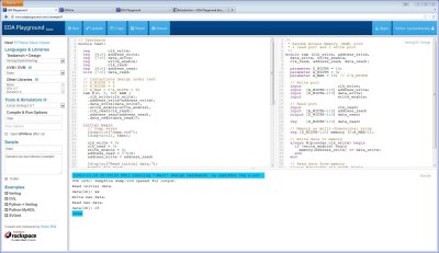
For part I, you need a Verilog simulator. I’m going to use EDAPlayground because it is free and it will run in your browser. No software to set up and no worry if you use some crazy operating system (like Windows). If you have a modern browser, you are all set.
I know some people don’t want to work on the Web or don’t want to create an account (honestly, though, this will just be tutorial code and making up a disposable e-mail address is easy enough). If you just can’t bear it, you can run all the examples on your desktop with Icarus Verilog (using GTKWave to display the results). I just won’t be talking about how to do that. You can read the Icarus introduction if you want to go that route. I still suggest you stick with EDAPlayground for the tutorial.
For the FPGA tools used in Part III, I’m using the open source Icestorm tools. I tried using the Lattice tools and it was heartbreakingly difficult to get them installed and licensed. I’ll have more to say about that in part III.
About the Target Hardware
 The IceStick has a modest FPGA onboard. From its manual, it has the following features:
- High-performance, low-power iCE40HX1K FPGA
- FTDI 2232H USB device allows iCE device programming and UART interface to a PC
- Vishay TFDU4101 IrDA transceiver
- Five user LEDs (one green and four red)
- 2 x 6 position Diligent Pmod compatible connector enables many other peripheral connections
- Discera 12Mhz MEMS oscillator
- Micron 32Mbit N25Q32 SPI flash
- 16 LVCMOS/LVTTL (3.3V) digital I/O connections on 0.1” through-hole connections
The FPGA isn’t huge, but it is big enough to host a simple CPU (we covered the CPU earlier). We aren’t going to start with a CPU, though. We’ll start with something much more simple.
Let’s Build an Adder
There are two main kinds of circuits you build on any FPGA: combinatorial and sequential. The difference is simple: combinatorial logic is all logic gates. The past state of the circuit doesn’t matter. Given a certain set of inputs, the outputs will be the same. A sequential circuit (which almost always has a flip flop in it) has some memory of a previous state that changes the output. I wanted to show examples of both and how you map them to the board.
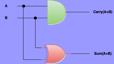 The example circuit we’ll build has three major parts. The first is a two-bit adder circuit that shows a binary sum and carry on two of the board’s five LEDs. This is a simple combinatorial circuit. It doesn’t make use of the onboard 12MHz clock. The other two portions will. The first sequential circuit will be a simple memory that latches true if a carry has ever been generated by the adder (after a reset, of course). The other sequential circuit is a set of counters that combine to provide a 1/2 second pulse from the 12MHz clock.
Verilog Versus Schematic Entry
For simple circuits, it is tempting to just draw a schematic like the one above and either machine translate that to the FPGA or hand translate it to Verilog. Some tools support this and you may think that’s the way to go. I know I did when I got started.
The truth is, through, that after you move away from simple things, the schematics can be very painful. For example, think of a seven segment decoder. If you took a few minutes you could probably work out the AND OR and NOT gates required to perform the function (that is, convert a four-bit binary number to a seven segment display). But it would take a few minutes.
If you use Verilog, you can take a simple approach and just write out the gates you want. That will work, but it is usually not the right answer. Instead, you should describe the circuit behavior you want and the Verilog compiler will infer what circuits it takes to create what you need. For the seven segment decoder this could be as simple as:
always @(*)
case (number)
 4'h0: dispoutput <= 7'b1111110;
 4'h1: dispoutput <= 7'b0110000;
 4'h2: dispoutput <= 7'b1101101;
. . .
I promised I’d point out some of the stranger points of Verilog, so let’s look at that in a little more detail. The always statement tells Verilog that the code following should execute whenever any of the inputs you use in it change. This infers a combinatorial circuit since there is no clock. The case statement is like a switch statement in C. The funny looking numbers are four bit hex (4’h1) and 7 bit binary (7’b1101101). So the code instructs the FPGA (or, more accurately, the Verilog compiler) to examine the number and set dispoutput based on the input.
The <= character, by the way, are a non-blocking assignment. You could also use an equal sign here to create a blocking assignment. For now, the difference doesn’t matter, but we’ll revisit that topic when working with a sequential design.
From this description of what you want, the Verilog compiler will infer the right gates and may even be able to perform some optimizations. A key difference between an FPGA and building things on a microcontroller has to do with parallelism. If you wrote similar C code on, say, an Arduino, every copy of it would take some execution time. If you had, for example, 50 decoders, the CPU would have to service each one in turn. On the FPGA you’d just get 50 copies of the same circuit, all operating at once.
Key Verilog Point #1: Verilog isn’t Executable (Except when it is)
That’s a really important point. With an FPGA, the circuitry that drives each display just works all the time. Sure, there is a small delay through the gates (probably picoseconds) but that’s true even with discrete circuitry. It isn’t because the FPGA is executing lines of Verilog code or some equivalent structure. The Verilog becomes connecting wires that wire up circuit elements just as though you had a sea of gates on a PCB and you connected them with wire wrap.
There is an exception to this. During simulation, Verilog does act like a programming language, but it has very specific rules for keeping the timing the same as it will be on the FPGA. However, it also allows you to write constructs that would not be transferable to the FPGA. For example, a subroutine call doesn’t make sense in hardware, but you can do it during simulation. In general, you want to avoid non-synthesizable Verilog except when writing your testbench (the driver for your simulation; I’ll talk more about it in a minute).
Look back at the adder schematic. The sum is a simple XOR gate and the carry is an AND gate. I can express that in Verilog, if I want to, like this:
assign carry=inA&inB;
assign sum=inA^inB;
It is smarter, though, to let Verilog figure that out. I can make a variable with two bits in it like this:
reg [1:0] fullsum;
Then I could say:
assign fullsum={1’b0, inA} + {1’b0, inB};
assign carry=fullsum[1];
assign sum=fullsum[0];
The braces turn the one bit wires inA and inB into two bit quantities. In this simple example, I might have actually stuck to the first method, but if you think back on the 7 segment decoder, you’ll see it makes sense to use this inferring style where possible.
Modules and Definitions
When you watch the video below or browse the code, you’ll notice there’s a few minor things I glossed over. For one, all of this code lives in a module. You can think of a module loosely as a subroutine or, better, a C++ class. Other modules can create copies of a module and map different signals to its inputs and outputs. There’s also definitions of all the nets used (we already talked about wires and regs):
module demo(
 output LED1,
 output LED2,
 output LED3,
 output LED4,
 output LED5,
 input PMOD1, // input A
 input PMOD2, // input B
 input PMOD3, // run/stop
 input PMOD4 // reset
 );

// Alias inputs
 wire inA;
 wire inB;
 assign inA=PMOD1;
 assign inB=PMOD2;
Note that I wanted the signals to have names associated with the physical hardware (like LED1 and PMOD2) but then later I wanted to use more meaningful names like inB. The assign statement makes this connection. This is a simple use of that statement. If you recall, one way to build the adder was to assign two bits using an expression. That kind of usage is far more common.
A Test Bench Makes The Simulation Possible
Before you commit your design to an FPGA, you’ll probably want to simulate it. Debugging is much easier during simulation because you can examine everything. When the Verilog simulator runs, it follows rules about timing that take into account how everything runs at the same time, so the behavior should be exactly what your FPGA will do.
The only thing many simulators won’t do is account for things like timing on the chip itself (although with the right tools, you can simulate that too). For example, your design may depend on an input changing before a clock edge (the set up time on the flip flop, for example) but because of the routing on the chip, the input won’t change in time.
This kind of timing violation is a real problem with large chips and high speeds. For this sort of small circuit, it shouldn’t be an issue. For now, we can assume if the simulation works, the FPGA should behave in the same way.
To test our code, we need a testbench which is just a way to say a piece of Verilog code that works like the outside world to our unit under test (in this case, the whole design). The code will never synthesize, so we can use strange Verilog features that we don’t normally use in our regular code.
The first thing to do is create a module for the testbench (the name isn’t important) and create an instance of the module we want to test:
`default_nettype none
module tb;
 reg  a, b;
 wire led1, led2, led3, led4, led5;
 demo dut(led1,led2,led3,led4,led5,a,b);
Note that there is a reg for each input we want to feed the device under test and a wire for each output it will drive. That means all of those reg variables need to be set up to our test conditions.
The variables need to be initialized. Verilog provides an initial block that is usually not valid for synthesis, but will be the main part of most test benches. Here’s the first part of it:
 initial
 begin
   $dumpfile("dump.vcd");
   $dumpvars(0, dut);
   a=1'b0;
   b=1'b0;
The two $ statements tell the testbench to dump variables from the device under test to a file called dump.vcd (this is where EDAPlayground looks for it, too, so don’t change it unless you are using your own Verilog simulator). We’ll be able to examine anything that gets dumped. You can also print things using $display, but I didn’t do that in this test.
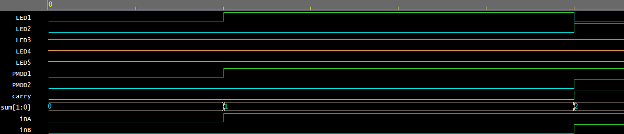
The next thing you need is some test case stimulus. In the case of the counters, you don’t need anything other than the clock. But the adder-related circuitry needs some values:
#2
 a=1'b1;
 #4
 b=1'b1;
 #4
 a=1'b0;
 #4
 b=1'b0;
 #4
 $finish;
 end
So at first, a=1 and b=0. Then after 4 cycles, a=1 and b=1. After another 4 cycles a=0, b=1. Then a=0, b=0. The $finish statement causes the simulation to end. Without this, the clock generator will cause the simulation to keep going forever.
You can find the code and the testbench on EDAPlayground (you can even run the simulation from there). When you run the simulation, a waveform will appear (see below). If you want to know more about how it works, check out the video below and I’ll walk through it step by step.
Next Time
In tomorrow’s installment of this series, I’ll show you how to add sequential (clocked) logic to the design and the testbench. Using clocks are an important part of making practical digital designs, as you’ll soon see. I’ll also have a few more Verilog key points.
Selected Tutorials
If you are looking for a detailed Verilog tutorial, try these:
- Doulos (host of EDAPlayground) has a very professionally done set of tutorials
- Another tutorial set up as a self study course
- The creator of EDAPlayground has a series on YouTube that would be helpful, especially if you are using EDAPlayground


>> Key Verilog Point #1: Verilog isn’t Executable
This is probably the biggest hurdle to overcome when learning FPGAs. Once you make that leap to thinking in terms of a hardware description rather than an executable language it all falls into place (at least it did for me).
Life’s too short to pick up bad habits. Just write:
always @(posedge clk)
count <= count + 1;
You are jumping ahead! I haven’t talked about clocks yet. Besides, what I’m building here isn’t a counter. It is an adder. But hang on… it is all coming….
I was referring to the “verilog tutorial 1” that comes up at the bottom of the page, with the ripple carry counter example.
I have a few FPGA boards and CPLDs laying around growing a layer of dust I need to get around to playing with.
I kind of (but vaguely) get the idea that you are more “building logic circuitry” in software than programing software to run on some hardware, and rather than things running sequentially as you would expect with software, they should be running parallel, as it is more like true hardware. But just thinking about it makes my head spin.
BUT the biggest hurdle I have is getting my head around the software you use to program these damn things! Altera Quartus and I’m sure all the rest are beasts to understand, for me anyway. And I’ve used quite a few IDEs.
“If you know C you can pick it up quickly” is a bit of an understatement. 8)
Maybe “If you know C, and you code without any blocking functions, and you don’t use dynamic memory allocation, you don’t use recursion, you only use loops that can be unrolled flat at compile time, and you are comfortable with all your variable assignments occurring atomically over the whole program, then you can pick it up quickly” would be a little closer to the truth.
It’s not even about blocking functions in the C/Posix (or other api) sense. You are designing around what can be done in a clock cycle & number of gates required. So, a simple loop can do the minimum required to make progress in a tick, or a big combinatorial circuit that would calculate multiple iterations at a time (assuming no dependence on the previous iterations). The big circuit might not even be worth it if the propogation delay through the circuit wasn’t significantly faster than the iterative state-based version when you consider the cost of moving up to a part with more logic elements.
I got a passing sense of this working with an FPGA guy prototyping an accelerator for elliptic curve cryptography, and it was pretty enlightening. The tradeoff between sequential and parallel computation was made very obvious by the time our designs made it through synthesis (generation of logic from VHDL) and place and route (positioning of logic on the fabric).
Part of me wishes I could quit my job and do some logic design in anger. I’ve got a background in formal methods (i.e. machine checked proofs of programs), and working at that level made things real for me.
Ha. My ‘personal’ revelation to this conversation is in ancient days as an undergrad my first, primary degree was in Philosophy which included a required course in logic– Perhaps useful for the construction of a proper argument (though much better, I think for taking one apart).
Only toward my total shock, starting in on Verilog/FPGA’s– ‘truth tables (!)’– Oh how I never thought I would ever again see you/use you.
Towards Mike’s comment, after spending some time, the ‘syntax’ is like C, but the methodology is certainly not– Or as a paradigm, it reminds me of growing up with ‘linear’ programming and then the invention of OOP.
My personal feeling is that FPGA’s are *essential* in our modern computing environment (less you are a ‘big boy’ and can hash out, design an ASIC and even then), but I think they are really hard to get into only because the first question is just ‘why ?’.
However, plug around long enough and you will discover a problem/project that can not reasonably be solved in any other way, and it will be a ‘turn-on’ too–
I think the best way to start designing hardware is to draw a block diagram/schematic, and then translate it into a HDL. Depending on the skill, the block diagram can be more or less detailed.
Saying “it’s like C” seems like the wrong paradigm to understand hardware description coding.
If you really want to compare HDL code to something from the programming/CS domain, it might be helpful to think of it in terms of declarative programming – like say Haskell, or Prolog or something, even though it’s still not quite exactly the same paradigm – as opposed to an imperative language such as C.
Yes unfortunately with Verilog and VHDL you start in the deep end of the pool. Altera is perhaps the less vicious beast to tame so if your having trouble choosing, then start with Altera.
The truth is that all the IDE’s for this are hard to learn in the beginning. So it comes down to ‘when’ you start and not ‘what’ you choose to start with.
I bought a CPLD kit over 20 years ago and I could never register the software so I gave up, sadly. I only just recently tried again with Xilinx and Altera and I am so sorry now that I lost all that time due to one manufacturer (Vantis).
Also, the trial version of Sigasi is an excelent learning tool. It’s like a code editor but it instantly shows errors as you code.
The idea is that you are describing hardware. Verilog is a HDL aka “hardware description language”.
https://en.wikipedia.org/wiki/Hardware_description_language
and this is completely different from a software programming language in the same vein that blueprints for a building are different from the procedures and protocols surrounding getting people out of the building in case of a fire.
There is no software here beyond the programs / compiler running on your host operating system that allow you to take your hardware description through the process of synthesize, place and route, and transferring of the bitstream to the FPGA.
The Lattice Icestick FOSS toolchain referened in the article is quite easy to use. This was previously mentioned on hackaday at:
http://hackaday.com/2015/05/29/an-open-source-toolchain-for-ice40-fpgas/
http://hackaday.com/2015/07/28/open-source-fpga-toolchain-builds-cpu/
You can read and download the pieces of the project from:
http://www.clifford.at/icestorm/
The Cypress PSoc line has a small programmable logic section that you can target with Verilog. I’ve used it to build a quadrature decoder, and other pin driven state machines. Dev boards start at $4.
I have two of these (plus about $1000 worth of old 8051-based PSoC emulation hardware) but it pains me to bring up Windows just to code for them. I do like the chip, though. Just wish for better tool support on Linux.
What about VHDL?
Maybe a future topic. I do both, but given a choice I do Verilog. However, the key concepts are the same: you aren’t writing code, you are inferring circuits, etc. Note that EDA Playground will do VHDL if you want to experiment with no tool download/setup. However, I don’t think the iCEStorm tools we will use to program the board does VHDL (yet). The Lattice software surely does, but… I’ll tell you later… it is painful to download and install, especially under Linux.
According to my TA in university: America uses Verilog, Europe uses VHDL.
Conceptually they’re similar. VHDL is slightly more powerful but slightly more difficult to use. If Verilog were C++, VHDL would be C. Designs often start as Mealy/Moore machines scribbled on paper during meetings, so syntax is just implementation.
Now if only I could find a useful application for the Virtex-II that I found in a scrapyard, I’d have a reason to get back into FPGA development. FPGA design in HDL and embedded programming were some of the most enjoyable parts of my EE degree, but the Raspberry Pi came out shortly after I graduated, and I’ve been able to do most of my projects using that. Most projects only get to the demo stage anyway.
If you have ideas of how I could use a Virtex-II with two RS232 I/O ports, two ADCs, two DACs, some DIP switches and LEDs, I’m very interested.
Verilog is like C
VHDL is like COBOL
VHDL was developed for a US military project…so it’s public domain, unlike Verilog, but you get what you pay for :-)
Actually, VHDL is like Ada.
“Look back at the adder schematic. The sum is a simple AND gate and the carry is an XOR gate. I can express that in Verilog, if I want to, like this:”
@Al hey your logic is backwards in this statement. The sum is the XOR gate and the carry is the AND gate. I think you just flipped the roles accidentally.
Yep just a slip of the pen. It is right in the Verilog and the drawing. Fixed in a second–thanks!
Please, before you start adding in clocks and wondering why things don’t always behave as you expect, you need to be aware of how Verilog processes lines and the use of blocking and non-blocking assignments.
always @(*)
case (number)
4’h0: dispoutput <= 7'b1111110;
[etc]
Should really be written:
always @(*)
case (number)
4'h0: dispoutput = 7'b1111110;
[etc]
(then inside any clocked statements, those with always @(posedge clk), use the non-blocking assignment of <= )
Yes, that comes up in the next segment which is already scheduled. The tools will correctly infer the right assignment in a combinatorial block regardless of how you write it, though, especially where there’s only one like this. The rule of thumb about using = vs <= in a block like this is due to simulation performance. I had originally had the discussion of = vs <= in this part, but it was just too long so I split it, and that wound up in today's installment.
You just have to careful not to mix them up, because that can generate some unexpected results, where simulations don’t always agree with hardware. For me, that’s a good reason to try to be consistent, even when it’s not strictly needed.
The simulations and the hardware will agree when you use <= or =. The issue is your expectations. Again, I'm trying not to do part 2 in the comments, but the semantics are well defined both at simulation and synthesis.
While I appreciate that it can work in simple examples, it was more of a “how to learn” step – even if you’re not going to explain some of the subtleties, you should really teach ‘best-practice’ (even if you don’t initially explain why it’s like that and not another form).
My desire for getting them right, is down to the Verilog evaluation process as it leaves non-blocking until the end of the process cycle, whereas blocking can be continually re-processed within the cycle if any signal within the sensitivity list changes and this can (*cough* has) caught out unsuspecting users in larger simulations with “zero-cycle” issues.
(If you want to start looking into performance then you’d be interested to hear that, about 7 years ago, colleagues of mine discovered that if one wrote reset terms for an active low registers ran using !reset_n rather than ~reset_n, they ran faster.)
ICE seems to be verilog biased, all the libs for ICE FPGA are readily available in verilog, for VHDL demos I had to write my own wrappers.
https://hackaday.io/project/6636-iced-an-arduino-style-board-with-ice-fpga
when I was making test code the the ICEd board, it is by the way mostly compatible to the ICEstick, so many designs for ICEstick also run on ICEd without any changes.
I have the ICEstick and the mystifying thing is, they have a device with 144 or more pins (haven’t checked the package) and only bring out about 30 pins to pads. Seems a terrible waste just to look like a thumb drive form factor.
That’s the first thing I thought when I saw it – qfp144 and next to nothing broken out.
Hi,
Interesting article.
Id there a code fragment missing? I can’t see the code where #1 is, only #2….
“In English, this says: At all times, you should delay one clock cycle (the #1) and then invert the clock signal and keep doing that forever.”
Cheers
Bryan
Oops. That is an artifact of having split the piece into two. So if you look at part 2, you’ll see that part. Nice catch. I’ll remove it from here.
Al, are you aware of Logisim? (http://www.cburch.com/logisim/index.html) It’s an interactive graphical logic simulator, used in a lot of university design courses. I’ve used it for a few small projects but you can find complete CPU designs (on Youtube, of all places!).
Yes, I’ve seen it. However, the author pretty much stopped development on it in 2014–not that it isn’t perfectly usable. It is a wonder no one has forked it and taken it further.