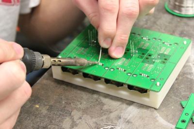
In our last installment of Tools of the Trade, we had just finished doing the inspection of the surface mount part of the PCB. Next in the process is the through hole components. Depending on the PCB, the order may change slightly, but generally it makes more sense to get all the SMT work done before moving to the through hole work.
Through hole used to be the standard, but as the need for size reduction and automation increased, SMT gained favor. However, there are still a lot of reasons to use through hole components, so they aren’t going away entirely (at least not any time soon). One of the biggest advantages of THT is mechanical strength, which makes it better suited for connectors than SMT. If you’ve ever popped a microusb connector off a PCB by breathing on it heavily, you’ll understand. So, how do we most efficiently get through hole components on a PCB, and how do the big boys do it?
By Hand
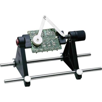
This is how most people start, and is still surprisingly common even in mass production. One of the tools involved is the helping hands, which can hold your PCB while you solder. These can get cumbersome quickly, though, so the next step up is dedicated PCB holding tools, which have rails and slotted rubber pieces that hold the edges of the PCB.
One problem with both of these, though, is that you generally have to put the component in on one side and solder it on the other side, so components have a tendency to fall out when you flip the PCB over. There are lots of ways around this, from bending the leads as you insert (or opposite corners on DIP packages), to soldering briefly on the top side to tack it on, then finishing on the other side.
Others have gone with more creative solutions, including the bed of nails approach, or foam that holds the parts in place while the PCB is flipped over and soldered by hand.
Sometimes you need to stand off a component from the board, and it has to be the same height off the board. In this case, one option is to use a standoff around one or multiple leads. Another is to design a jig that acts as the negative of the PCB. It is machined or 3D printed, and then the jig is placed over the PCB. When the pair is flipped over the components drop down to the correct height (or stay where they are), and can be soldered by hand.
Automatic Placement
Surprisingly, there are tools that automate the placement of through hole components. Or maybe not surprisingly, if you consider LED panels. These outdoor signs use through hole LEDs, and some quick math leads one to the conclusion that automatic placement of LEDs is a necessity.
Some LEDs come on strips of tape and a machine cuts the leads at the tape and places the LED where it needs to go. Lots of LEDs come in bags, though, and are placed in a hopper, which spins and spits out a line of LEDs, all oriented in the right direction. In either case, the LED makes it to a gantry which cuts the leads and places the LED in the holes. The same is done for resistors or other axial lead components.
Solder Pot
Imagine a coffee-mug sized container with a heating element around it. Then put a bar of solder in it. No flux, just a block of solder. Heat it up until it melts, and you have a solder pot. This is good for dipping the edge of a PCB in (not all the way, just the bottom) to get the pins of a connector to solder. You need to coat the PCB with flux first, because there isn’t any in the solder pot. This method is great for certain volumes and sizes, where you may only have one or two connectors that need to be attached to an otherwise completely SMT PCB, but if you want to do a bunch of connections on a larger PCB, you’ll need to use a wave soldering machine.
As a side note, solder pots are also great tools for recovering components from PCBs, since they can heat up the whole component quickly from the underside, making it easy to remove, clean, and with minimal danger of overheating the component.
We’ve covered dangerous homemade solder pots before, but you should probably just buy a used one if you want.
Wave
The wave soldering machine takes molten solder and pushes it up through a long channel with a pump so that there is a long thin fountain of solder coming up a few millimeters. Then the PCB is dragged along some sort of conveyor so that the fountain just touches the bottom of the flux coated PCB, and the wave instantly attaches to the through-hole pads and pins and makes the connection so beautifully. This is an easily automated process, provided the bottom is clear of components. If there are components on the bottom, they will need to be masked first.
A bastard child between the wave solderer and a solder pot is the dip solderer. You put your PCB on a metal frame, and the frame dips down onto a molten sheet of solder until just the bottom is touching the solder, and then it is raised up. It’s a pretty simple mechanism that doesn’t take up a lot of space, but the boards still need to be coated underneath with flux.
Conclusions
There’s still a place for through hole, and even in mass production it’s very common. While the world is moving towards surface mount, there are still perfectly legitimate reasons (connectors and high power applications especially) for using through hole. It’s particularly easy to do by hand, and as production scales there are some tools that make it easier. We haven’t seen a homemade wave soldering tool yet; solder pots are about the extent of DIY tools for mass production of through hole parts, but they’re perfectly capable of handling pretty large volumes.


I get the point re the validity of through-hole in modern tech, but this article still feels a little 2005 in its wording.
Get the fuck out of here, 2016 2016 2016.
Better?
I heard a story about a shop that was trying to set up their new wave soldering machine for a short parts run, and didn’t want to melt a whole potfull of solder. So they tossed a brick into the solder reservoir and switched it on. It wasn’t until the solder melted that they remembered that bricks floated on lead…
Heh, and everything that doesn’t is more expensive I think.
I still cave-man my TH connectors. I hold them and the board in one hand and the iron in the other. The end from a solder spool hangs in mid air and I tack one pin down that way. I then inspect the fit and adjust if necessary and repeat for the rest of the connectors. When all that’s done, I set the board down and solder the rest of all the pins.
So I guess that holding solder between my teeth, as a third hand, should be considered quite primitive… :-)
That’s not good for you man. A lot of solder has lead, and flux is bad for your lungs, and other open tissues like your mouth.
Lead damages the kidneys, increases blood pressure and damages the nervous system including the brain.
Once lead is absorbed into the body it never comes back out. I alters the chemistry of the brain causing cognitive problems in adults and developmental problems in children.
Have you ever heard of the phase “Mad as a hatter”. A hatter was a person who shaped hats by immersing them in mercury and manipulating their shape. This exposed them to high doses of mercury which like lead does not come back out of the body and influences brain chemistry and driving them “Mad” as in exhibiting unpredictable behaviors that would today be describes as being psychologically unstable even though the cause is neurological.
That’s why we have RoHS lead free solder now. I still use lead solder as it’s too late for me now lol – been mad for years.
The funniest RoHS lead free product I have seen it lead-free car battery terminal connectors.
For a short time in the early 1990s, I worked at a place that repaired consumer electronics but also assembled circuit boards. For the assembly department, they had a few interesting contraptions: all the parts were in a machine what I can only describe as a “stacked carousel” of bins. Each layer of parts bins had one missing bin (think pacman) and the machine would rotate one of the carousel layers so that the part that was needed was towards the front. All the other layers had they missing bin towards the front, so it was easy to get the right part from the entire machine with hundreds of parts without mistake (if the machine was set up correctly of course).
The workers would sit at a desk with that carousel on it, and with a PCB that was exactly aligned, and held up in the air somehow (I don’t remember exactly how), and there was a “projector” that would shine a rectangle of light at the exact spot where a part had to go. The machine would adjust the rectangle to the right size. A computer controlled both the projector and the carousel, and there was a pedal on the floor that the worker could tap to let the computer know they were done with a part, so it could rotate the part bins in the carousel and adjust the beamer. When an entire PCB was done, they would put them in special adjustable racks that would be stacked up and saved for wave soldering later.
They didn’t have to cut the wires off AFTER placing them: there were special tools to bend and cut the wires BEFORE they were put into the parts bins and then onto the PCBs. Some of them were handheld, others were desk mounted. I remember the desk mounted ones had counters. The workers could look up in a table how many parts of a certain type they needed and how they needed to be bent and cut, and they could adjust the cutter to the exact dimensions, and run a roll of resistors through it, monitoring the counter so they would have the exact right count.
I thought it was quite a neat system for placing through-hole parts. Clearly the only thing that was missing was a robot that was precise enough to put the parts onto the PCBs; they still needed humans for that (usually some young girls with small hands doing the work as a temp job until they went nuts and left). Unfortunately I can’t find any pictures online of the machines I’m referring to.
===Jac
We had those machines at a CM I used to work at including the machine that would cut the leads to a certain length. I was apparently the only engineer who did electronic projects at home and from time to time the inventory people would drop off a bag of a few hundred LEDs, resistors or something when the operator set the lead length wrong.
We only had a few of the carousel/projector rmachines. Most of the time we created 3-ring binders with pages of the board outline and silkscreen. We would use highlighters to mark all the similar parts. For example all the 100uF caps would be colored yellow, the .1uf caps blue, 1K resistors green, etc. Complex assemblies would have many pages.
At the bottom of each page the part number and number of those components used would be highlighted with the corresponding color. The assembler would then take that number of parts out of the bin and install them. That acted as sort of a checksum, helping to ensure the parts were inserted correctly, but not fool proof.
Some projectors could also indicate the correct orientation for polarized components.
Thru-hole… When you are to lazy to do point to point wiring:
http://youtu.be/xd3NPSV2DL4
Lazy – No!
Smart – Yes!
I especially like that all the parts enter the face plate from the same direction so that the face plate can be removed to replace a part without you needing to de-solder lots of other parts first.
Using the PCB text saves making decals or labels and that’s a lot of saved time as well. It also saves you having to deal with the rotational locking keys for switches and pots.
Yeah, I used to make them like this:
http://www.wolftronix.com/amc_control/index.htm
Much more labor intensive.
Damn, that is SWEET! It’s extremely easy to underestimate how time-consuming (and often messy) it is to do point-to-point wiring. Measure wire, cut, strip ends, tin ends, solder to component, apply heatshrink…..
The only problem with this sort of construction is that it’s best suited to situations where all the components can be attached from the same side of the panel. Not so good for, say, a mixture of switches (mounted from the rear/inside) and DIN connectors (mounted from the front/outside). For repair, you can’t then just loosen everything and remove the front panel.
Don’t forget selective soldering machines! A few assembly shops I’ve toured use these to do a handful of through hole parts on an otherwise SMD board.
https://en.m.wikipedia.org/wiki/Selective_soldering
So…… I’m the only one who has to hold soldering iron in my teeth to hold things with both hands?
Kidding, I don’t really do that……. very often.
Probably not a good idea because um, LEAD. Most cheap “third hand” devices are junk but the good ones will help as long as the PCBs aren’t large or heavy.
LOL… I just wrote the same reply !!! … And yes I touched the lead with my tongue.. it tasted like victory…. ;-)
I didn’t do this for a while, but in 90’s I did it regularly. Recently I did blood test for lead and was all ok. But lead would not be in my blood for now, it it’s already in the tissues.
OK, now how do they do boards with SMT parts on both sides?
Glue
Lest anyone think he’s kidding, he’s not.
Most folks familiar with SMD know that one of the Gerber layers is the paste layer for solder paste.
There’s also a glue layer. The glue layer lets you make a stencil for applying heat-set glue. The glue is used on larger SMD components too heavy to be held in place upside-down by the surface tension of the melted solder alone. Typically such parts have a designated area on them that is at the same elevation as the pads, but is not a pad. For example, SMA diode packages have such a spot between the two lands.
Actually, surface tension and adhesion does a pretty good job of keeping small parts (even relatively large SMT parts) attached on the underside. I’ve never used glue on our two-sided load boards… even for TSSOP8 or SOT223 parts. 0402, 0603, 0805, even really thick 1210s… no problem at all. Heck, I think even the big DO214AA diode has only fallen off once in 300+ boards… and that was a paste problem where there was nearly no paste on one end. 213 SMT parts on the bottom side of each board.
I still use lots of through hole parts for prototyping as it much easier to change or fix things when the inevitable happens.
I cheat though because I make the boards here and I hate drilling holes so I do things like bending the pin out on DIP so they can be surface mounted.
Is it just me, or does it look like Mr. Baddeley is missing todays technology we (in our company) have used for years and actually use today for 99% of our thru hole components?
You should look up THR, or thru hole reflow. Paste gets dispensed into the hole with the normal reflow stencil or direct paste deposition. Components gets picked from tape reel by robot, pushed into the hole, and the board travels down into the reflow oven with all the other SMD parts. Saves massive amount of time and cost in the production chain.
And there is the press-fit process, another technology we use widely for connectors and you did not write about at all. Basically you need a good board fab (drill tolerance), parts made to be press-fitted (pin design, tooling) and the tool.
We found out that wave soldering 96-pin DIN 41612 backplane connectors is a real pain (lots of rework needed), so we switched to a press-fit design. If you have delicate components you don’t want to (or should not) heat cycle too much, press-fitting connectors is the prefered solution if THR is not possible/available.
Hipsters? In my hackaday?
No way!!!!!!!!!!!!!!!!!
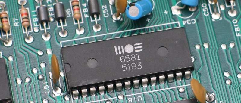
The shot of the MOS 6581 takes me back, I worked at Commodore/MOS the 51st week of 1983. I am assuming this is a C64?
It certainly is. The electrolytics and ferrite beads are a dead giveaway. http://www.mos6502.com/images/C64Internal/C64i_large.jpg
Who else did the stereo SID mod?
there are some flux’s that are slightly tacky and will hold Surface mount components down which might work with through hole. Personally, for through hole, especially when there’s a lot of them, I use painters masking tape. I’ll solder all the components that are roughly the same height, shortest first, then next shortest etc.