In part one, I compared the different Analog to Digital Converters (ADC) and the roles and properties of Delta Sigma ADC’s. I covered a lot of the theory behind these devices, so in this installment, I set out to find a design or two that would help me demonstrate the important points like oversampling, noise shaping and the relationship between the signal-to-noise ratio and resolution.
Modulator Implementation
 Check out part one to see the block diagrams of what what got us to here. The schematics shown below are of a couple of implementations that I played with depicting a single-order and a dual-order Delta Sigma modulators.
 Basically I used a clock enabled, high speed comparator, with two polarities in case I got it the logic backwards in my current state of burn out to grey matter ratio. The video includes the actual schematic used.
Since I wasn’t designing for production I accepted the need for three voltages since my bench supply was capable of providing them and this widget is destined for the drawer with the other widgets made for just a few minutes of video time anyway.
In Search of Digital Filters
 I also was attracted to the Cypress PSOC-5 as it had all of the components that make up the modulator plus they have a digital filter component that can be instantiated and programmed. Alas, it was a Finite Impulse Response (FIR) type which, although more common, isn’t a Cascade Integrator Comb (CIC) filter which we need.
This looks to be a cheap and powerful way to get exposed to digital filters and includes a workbench for generating the mathematical coefficients that drive a filter. I also wanted to show different ways to generate the coefficients, but simply ran out of time and space. I see a Hackaday post about FIR and other digital filters in the future.
Standalone Module
Ultimately I chose to use a standalone Delta Sigma Modulator IC AD7403 made by Analog Devices as a clean example of what I am trying to demonstrate. (While writing this post I learned that Analog Devices just acquired Linear Tech which scares me. I like the diversity of competition and still pine for the days when I would pull down a databook for Precision Monolithics, Elentac, or Intersil depending on what I was up to. I also miss National … a lot.) But back to our modulator…
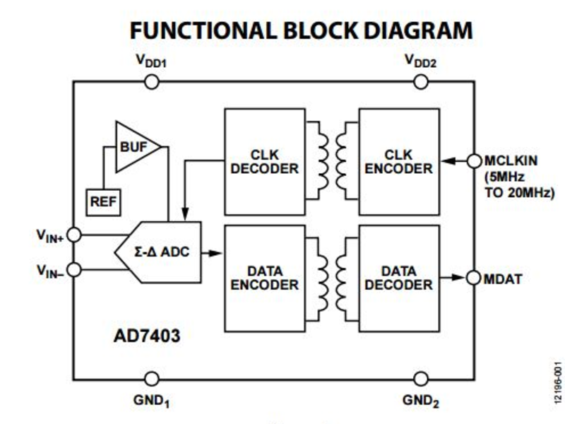
This particular module also has a cool feature in in that the ADC portion of the chip is isolated from the digital output portion, so much so that there are two sets of power pins including two grounds with no connectivity between them. This is useful in instrumentation or automation where the isolation is used to protect the digital back end equipment from the hostile environment the sensors are exposed to. As an example, picture shorting 480 Volts to an analog signal and NOT blowing out the computer that processed the signal from the ADC. Someone had previously asked about the isolation implied by the 4-20ma current loop standard, this is an example of a part you might use to achieve that isolation.
Modulator Output
Once again looking at the modulator output we see the single bit representation of the original signal, and then the oscilloscope reconstructing the signal by averaging.
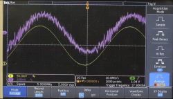
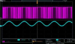
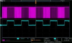
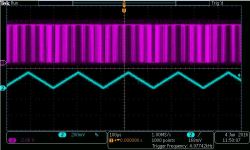
Averaging actually performs a similar function to the first step of the digital processing we need to do. Looking at the block diagram just below in the DSP section, what we need to do is accumulate a bunch of samples, and then thin them back down, or decimate them, to just what we need. The act of integrating allows us to accumulate the positive effects of oversampling and also provides the noise shaping, resulting in two noise reduction techniques right off the bat.
Sample Rate Conversion
As an aside, having an averaging/integrating function followed by a decimating function is basically how sample rate conversion works. For example converting from the audio CD standard of 44.1K samples per second to the DAT/DVD 48k rate, the 44.1ksps is first accumulated (multiplied) by a value of 160 and then decimated (divided) by 147 to get the end result of 48k.
Digital Signal Processing (DSP)
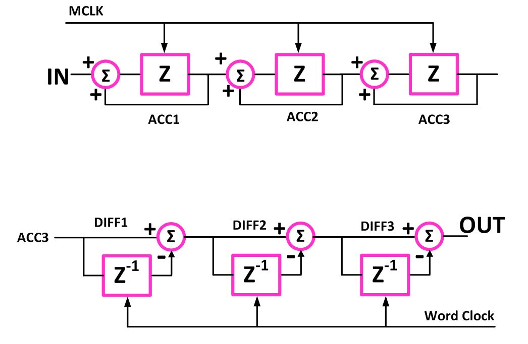 Here is a block diagram depicting the stages of the CIC filter. This is fairly standard way of depicting the operations in DSP-speak, the summation blocks show simple adding and subtracting and the blocks marked Z are basically clocked register storage. You can see that a series of these registers is a pipeline of intermediate results with operations between them.
A lot of DSP implementations work this way, there is an inherent delay in getting the first result as it has to clock its way through all of the stages but then an answer is available on each subsequent clock. That is, there is usually some latency but also high throughput when using pipelined architectures.
CIC
Looking at the block diagram, one of the advantages to using a CIC filter over slightly more complicated filter topologies is that there is no multiplication or division needed, just addition and subtraction. Multipliers and dividers require more hardware to implement in hardware, just as there would be more instructions needed for multiplication if implementing in software.
It should be noted that the CIC function here can be implemented in software, with the difference being that it takes many processor clock cycles to yield a result. The hardware DSP provides a value every clock cycle. There are other inherent differences between hardware and software implementations of filters in general, and arguing about them has passed many an hour at the local bistro.
DSP in FPGA
 One of the topics here at Hackaday is asking what FPGA’s are good for given the versatility, performance, availability and price of microprocessor or microcontroller based hardware. Digital Signal Processing is one area were once you step up to an FPGA implementation you may have lots of options such as multiple conversions in parallel or complex functions that still provide an answer every clock cycle.
I found many examples of CIC filters written in Verilog and VHDL on the net but a straightforward example was included right in the datasheet for the AD7403. They even include the block diagram which matches ours. I cleaned up some of the typos in the Verilog as there was probably an OCR step somewhere along the way in the creation of the datasheet for AD7403: CIC Filter in Verilog.
This file is now the basic building block of our CIC filter and can be used in any of the available FPGA design suites. As I have my Altera Quartus already loaded and a target board with a Cyclone IV handy so I will be using Quartus. Quartus has a free to use version which is close enough to open source for me and it includes the powerful ModelSim simulator . I swear I will try and get to a Lattice version some time when I am not already behind schedule.
Create the FPGA Project
 Step one was to create a project directory and save a copy of the CIC filter text file written in Verilog there. The next step was to run the New Project Wizard and select the EP4CE6E22C8 which is a 144 Pin version of a Cyclone IV on my target board.
Next I imported the pin assignments I have made for this particular FPGA development board, though I didn’t really use of the static pin assignments in this exercise other than the global clock. <Assignments, Import, Select file>
Next is to add the Verilog file to the project. <Files, Add File to Project, select file>
Design Top
 A personal preference of mine is to work with a graphical top sheet for a design and show the pins and files as interconnected blocks. This allows me to easily visual pin assignments, add simple inversions or other intuitive logic, and also add test points or other temporary functions that I can then remove later.
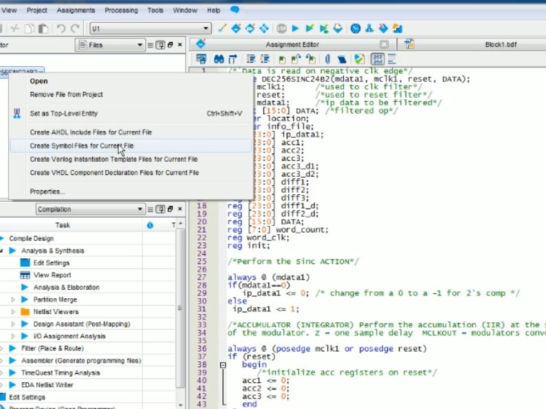
To do this with a Verilog file I create a symbol file for it for use in the top level graphical sheet.which compiles the Verilog file and if successful, creates the symbol.
Insert the Block
The final steps consists of inserting the block <Insert, Symbol, select file>, and placing it on the sheet. A quick shortcut provided by using this method is that I can auto-generate the pins by selecting the symbol and then <Generate Pins for Symbol Ports>. 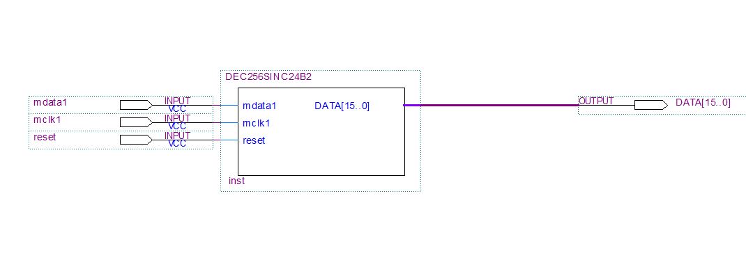
I can then optionally assign pin numbers if I want or I can let the compiler create pin assignments. Letting the compiler decide on pins is often not possible late in the design cycle when consistency is needed, however allowing the compiler to select assignments and other resources during an initial pass often can yield a more optimized use of FPGA resources.
Connect, Compile and Program
That’s it for creating an FPGA design from a HDL file assuming that there is no optimization or debugging needed. The next steps are to do the final compilation and program the part. <Processing, Start Compilation> <Programmer, select file, Start>
Using a Wizard to Make a Filter
Quartus includes a library of high-level components such as DSP filters that you can use for free as long as the programmer is plugged in to the development board. I know that Xilinx includes similar features in their design suites but I haven’t used them recently enough to say more.
So in essence we can build a CIC DSP filter without writing a single line of code. Open the system builder Qsys <tools, qsys=””> . The CIC filter can be installed by opening the Library from the IP Catalog and under the DSP heading select CIC under Filters. On the right hand side the various parameters may be selected to create the variation of the filter we are interested in.
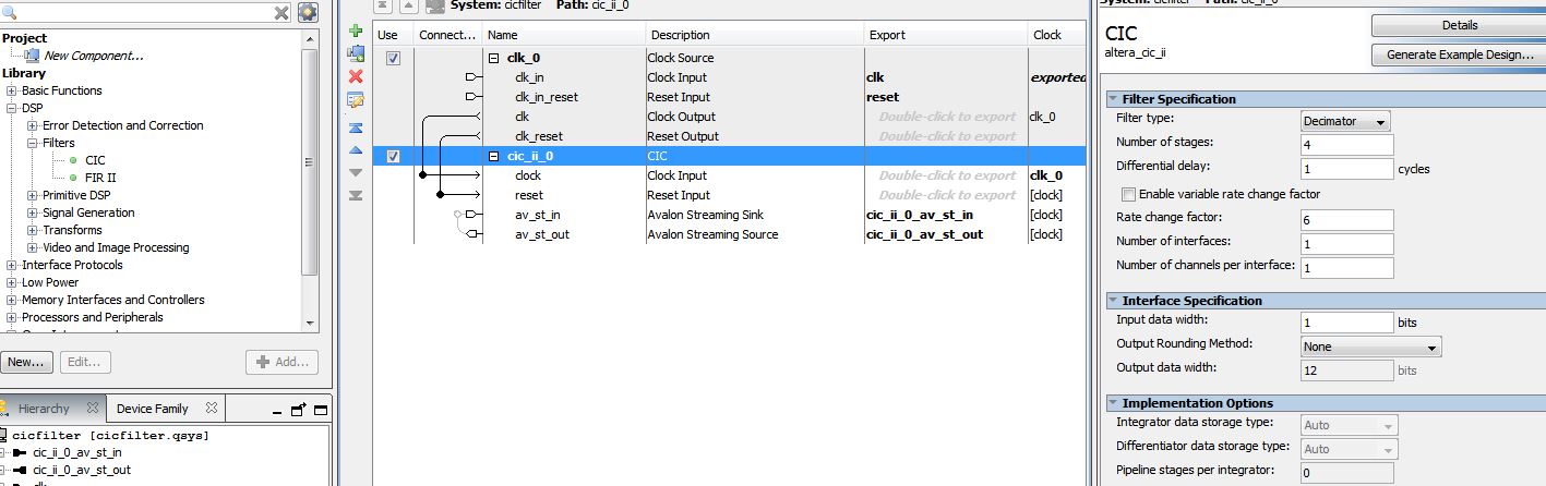
Finally we set up the interconnect and export the inputs and outputs as ports (best to watch the video for this part) and click <Generate HDL>, select <Verilog> and then click . As the box was checked we will get both the Verilog text file and a symbol as we did in the previous example.
From here it’s just like the previous example, you instantiate the symbol representing the Qsys design and hook it to pins, compile and program.
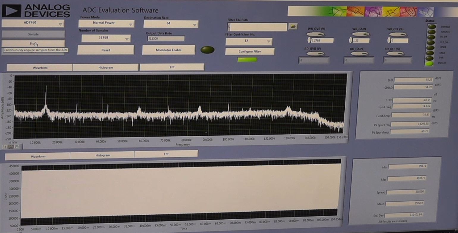
AD7760 Evaluation Board
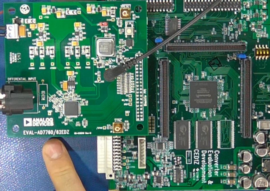 And finally I wanted to show some interaction with some of the variables such as decimation rate and average size. Using a development board and a motherboard made to couple to it I am able to display the output of the AD7760 24-bit Delta Sigma ADC. The interface allows me to adjust the various parameters and observe them and then also display in real time things like the calculated Signal to Noise Rate (SNR) and the Total Harmonic Distortion (THD). Again I recommend checking out the video as this is somewhat interactive.
As a parting shot I select the modulator output in the frequency domain and there is our noise shaping that we know is built into the design of Delta Sigma converters.
Delta Sigma Omega
The Delta Sigma Analog to Digital Converter demonstrates a combination of technologies that works together to improve speed and resolution beyond what a single technique alone could achieve. It also benefits from both analog and digital noise reduction techniques in its role of bridging analog and digital domains.
Resources
- Analog Devices AD7403 Datasheet
- Principles of Sigma-Delta Modulation for Analog-to Digital Converters (Motorola)
- How delta-sigma ADCs work, Part 1 (TI)
- How delta-sigma ADCs work, Part 2 (TI)
- TSA002 – 16-bit Sigma Delta ADC Design
- FPGA based sigma –Delta analogue to digital converter design
- Exploring Decimation Filters
- Combining the ADS1202 with an FPGA Digital Filter for Current Measurement in Motor Control Applications
- Verilog Fundamentals
- CIC Filter Introduction
- Understanding CIC Compensation Filters (Altera)
- Demystifying Delta-Sigma ADCs
- TSP #32 – Tutorial on the Theory, Design and Measurement of Delta-Sigma Analog to Digital Converters – YouTube (Really good, includes the math)


Excellent article!
As an improvement on the Verilog implementation of the CIC filter, instead of creating a new clock, word_clk can be used as a clock gater enable and the last half of the design can still be clocked with mclk1.
/*DIFFERENTIATOR ( including decimation stage)
Perform the differentiation stage (FIR) at a lower speed.
Z = one sample delay
WORD_CLK = output word rate
*/
always @ (posedge mclk1 or posedge reset) //<- still using mclk1
if(reset)
begin
acc3_d2 <= 0;
diff1_d <= 0;
diff2_d <= 0;
diff1 <= 0;
diff2 <= 0;
diff3 <= 0;
end
else begin
if ( word_clk ) begin //<– clock gater enable here
diff1 <= acc3 – acc3_d2;
diff2 <= diff1 – diff1_d;
diff3 <= diff2 – diff2_d;
acc3_d2 <= acc3;
diff1_d <= diff1;
diff2_d <= diff2;
end
end
/* Clock the Sinc output into an output register
WORD_CLK = output word rate */
always @( posedge mclk1) begin //<– still using mclk1
if ( word_clk ) begin // clock gater enable here
DATA[15:0] <= diff3[23:8];
end
end
Yeah I am all about one master clock and then little tiny clock enable pulses, asynchronous clock typically are bad. In this case I presented as is
Thanks Nathan
of course then you’d want word_clk to be a edge detected pulse…
reg word_count_7_q;
always @( posedge mclk1 ) begin
word_count_7_q <= word_count[7];
end
always @ (word_count) begin
word_clk <= ~word_count_7_q & word_count[7];
end
in one neat line:
{word_clk,word_count} <= {1'b0,word_count} + 1;
Are any of these COTS boards? If so, what are they?
Delta-Sigma converters are everywhere as a built in function or a self-contained ADC with I2C interface. (When looking at cheap, small DS converters in Digikey’s selector, Adafruit’s assembly came to the top of the pile)
For playing with the DS Convertor and more analog (including a digital filter) the PSOC5 cost about $10 and is pretty cool.
The assembly I show at the bottom with the software costs about $500 total, too expensive for anybody not looking at characterizing a serious application.
Xilinx Vivado HL Webpack lets you write functions in C/C++ and it automatically converts to VHDL or Verilog.
The video is a bit old but it shows the process.
https://www.youtube.com/watch?v=yHUTok7Y6CQ
Cool, thanks. In really big functions converting from C type code to pipelined, parallel processing as found in FPGA can require lots of manual intervention by someone who understands the app and the FPGA at very high levels. I have some $200 books on DSP function tweaking that talk about nothing but how to optimize the net flow at the FPGA level.
Yeah, I’ve seen some projects and they’ve used a massive gate array, proudly state they’ve used 8000 nodes, and you figure it must be super complex, but then you dig into it and find everything was “done wrong” as it were assigning pins first, using high high level tools and ended up using 10 times the gates and having to spec a part 3x as fast as they really needed.
I haven’t used it enough to get an idea of how well resources are optimized. If it’s anything like a modern C++ compiler then you may not be able to do a better job by hand optimization. That said, a code review and keeping an eye on the resources at build time is always a good idea.
I agree on just C/C++ optimization for assy code. Unfortunately the automatic process of taking code written for a single instruction at a time (microprocessor) has a pretty far leap to implement as a parallel, pipelined flow of data using various onboard features such as multiply-accumulate and understanding onboard memory prioritizers/controllers, and other primitives/advanced IP etc. (I am think of big dedicated DSP functions out of habit, Hello World would work just fine I suspect.) At best the result is an approximation of what the C did, at worst it just sits and burps. :)
Most end up rewriting in Mathlab or similar starting with the math itself and letting it compile in a FPGA target environment using the actual primitives/IP’s present in FPGAs.
I have seen some multi-$10K utilities from companies like Mentor get pretty close. A friend of mine that used to write cell-phones for a living used to use one judiciously, but I know he was still Mathlabing his ass off.
Thanks Darren!
Unfortunately this is a completely different problem, C++ to HDL is nothing like C++ to machine code. The high level synthesis engine trying to do the C++ conversion to HDL has to extract the intent of your C++ code and generate a fine grained synchronous parallel process.
It is literally compiling C++ code into a logic circuit.
From a usage perspective I think they have a lot in common. It doesn’t have to extract your intent, you specify it.
In OpenMP, a pragma can be used to direct the compiler to use multiple threads on a for loop and tell it how to do the scheduling. I’m not going to look at the assembler output because I know that the Intel engineers are better at it than I am.
In Vivado, they call it a directive. I can select a C for loop, and insert an unroll or pipeline directive with a couple mouse clicks. The compiler reports all the resources used and gives a latency and timing analysis. I don’t write VHDL on a daily basis so it’s a far cry better than me trying to optimize it by hand.
I could be wrong on this, but, considering the architecture of the Delta-Sigma, the conversion is basically AC coupled, correct?
Since each one-bit conversion is basically “higher/lower” than the previous sample, you MIGHT be able to get an accurate DC value when it first turns on, but wouldn’t DC errors accumulate over time so that this is useless for getting DC values?
quite the opposite, it accumulates the error and corrects for it so over time it keeps getting closer and closer to the actual value
Hi Kevin, Looking at this in general I would note that there is a feedback loop that ultimately compares the signal to a vREF and so I would expect a lot of drifts to be canceled. With that said I have usually considered the Delta-Sigma to be an AC type of ADC mostly because I tend to reach for other converters at DC (Dual Slope).
And with THAT said, if I were to try an use/improve the Delta-Sigma in a near DC application I might add an input multiplexer and sample a ground and full-scale reference and do some back end math.
Outstanding presentation. Thank you very much.
Nice one Bil!
I must admit I LOL’d the moment you brought out the AD7760/62-EDZ + CED1Z combo – I have one of the latter collecting dust somewhere, but I’ve been using about 5 of the former to collect data for a while now.
It’s about the only sigma-delta chip with built-in filter that one can make *not* do a ringy FIR. I mean, it does by default, but one can either upload a FIR set that doesn’t ring, or use it in 12-bit modulator mode and do one’s own digital filtering on that.
(although it does come at you at 20 MHz, which makes it a bit of a challenge to keep up with).
Pretty much every other ’24 bit’ sigma delta ADC around won’t let you cut back the decimation, or change the FIR taps, which gets frustrating. (They all use FIR’s with taps that look like a sinc function: nearly brickwall frequency domain performance, but horribly ringy step response, you end up losing a lot of time-domain resolution by the time you’ve added your own filter to eliminate the ringing afterwards, because the decimation after the wrong filter means you can’t just ‘undo’ the wrong FIR taps with another one.).
I love the new AD740x chips though: I like the AD7405 the most (so far), since the differential logic IO it has tends to not emit noise right nearby where you don’t want it. (Especially relevant if you’re wiring one by ~10 cm hookup wires to an FPGA. Because a good differential logic pair has the condition that the sum of currents is a constant, so the logic switching states tends not to emit/be-susceptible-to interfering transient noise, and this also means the digital outputs aren’t upsetting the power rails nearby either, although that’s much less of an issue with the isolation. ).
I certainly agree about wanting a multiplexor built in for calibration though!
I’m thinking a little DPDT relay, then feeding to a (channel common) analogue switch chip to generate 0 -> neg FS -> pos FS -> neg FS -> 0 -> input sequence of steps on demand for calibration (and confirmation that the filters are all working as expected: settling nicely without ringing). The idea of the relay is that when left un-energised, the inputs just go directly to the signal source, which should reduce the possibility of introducing noise. This should be ahead of the all-important analogue anti-aliasing filter, which ought to have a minimum-phase response too, and should have a nice wide guard band between it’s -3dB point and 10 MHz (for a 20 MHz sample clock), since whatever it attenuates to at that point is going to bear a striking relationship to the final SNR one can pull out of it.
I have noticed that the difference between a cheap ~-60dB ’24 bit’ audio ADC and a more expensive ~-110dB one seems to be the -50 dB of rejection at half the sample rate the latter’s ‘recommended input front end circuit’ has.
Of course, there’s a whole ‘nother article in how one gets ~10 – 30 MB/s from multiple AD7760’s into a file reliably without a ~$1000 PciE dev kit. (hint: You should be able to do it very easily with the CED1Z, it has everything you really need for that: An ‘FX2’ hiSpeed USB2.0 fifo, and an FPGA with enough SDRAM to buffer for a couple hundred ms.
The cheapest dev kit with the same necessary parts I know is the DSLogic, which has about the same chipset, although with a Xilinx Spartan6. It’s very interesting that NI’s ‘Compact-DAQ’ USB capture system has the same too.)
PS: Try not to spend too much time understanding the FX2 – unless you really like ‘8051’s and complicated memory maps with built-in custom state machines with enough complexity themselves to handle ATA66 parallel transfers… Go get [fx2pipe](http://www.triplespark.net/elec/periph/USB-FX2/software/fx2pipe.html) and use that instead, with the chip in ‘slavefifo’ mode, 16 bits at 30 MHz wired straight to a FIFO block within the FPGA. Try to avoid having to use it to also configure the FPGA, it’s not worth the hassle. If you can’t avoid that, then ztex.de have a nice open source fx2 SDK which makes it comparitively easy to compile custom USB device firmware using sdcc. fx2pipe itself uses a slightly dodgy hack of blindly overwriting just a little of the default firmware in the fx2 to change slave fifo port settings, whilst leaving the default interrupt handlers etc alone. It works, and will do so with any fx2, provided it’s wired halfway sensibly.
PPS: FWIW A hardkernel Odroid-C2 with fx2pipe spewing data piped directly to netcat can push about 38MB/s over a gigabit ethernet quite nicely, in either direction. In fact fx2pipe seems to work very well on just about any arm SBC, except RasPi’s. They don’t really have anywhere to send the data to; if you’re already taking all the USB bandwidth, then there’s little left for the ethernet or mass storage. nc | dd with the right settings somewhere else can then catch that data and throw it into a file.
CIC filter is allready in ADC_DeltaSigma block
quote from PSoC creator component datasheet:
The ADC_DelSig is composed of three blocks: an input amplifier, a third-order delta-sigma modulator, and a decimator.
…
Decimator block contains a four-stage CIC decimation filter and a post-processing unit.
Yup, that component is a complete component. I had been looking at making the modulator out of the (internal) discreet OpAmp and switch components (with external cap for integrator) and then using an internal digital filter. I.E. make a DS ADC without using the on-board DS ADC.
I am implementing a Delta Sigma Modulator using Cyclone II DE II. I am sampling a 10KHz sine input with a 100KHz clock. I need a CIC filter at the output with a rate decimation factor of 5 at the output. Can you please explain what should be the modifications done for the verilog code
module cictestingad
(
input mclk1, /* used to clk filter */
input reset, /* used to reset filter */
input mdata1, /* input data to be filtered */
output reg [15:0] DATA, /* filtered output */
output reg data_en,
input [15:0] dec_rate /* Decimation Rate */
);
/* Data is read on positive clk edge */
reg [36:0] ip_data1;
reg [36:0] acc1;
reg [36:0] acc2;
reg [36:0] acc3;
reg [36:0] acc3_d2;
reg [36:0] diff1;
reg [36:0] diff2;
reg [36:0] diff3;
reg [36:0] diff1_d;
reg [36:0] diff2_d;
reg [15:0] word_count;
reg word_clk;
reg enable;
/*Perform the Sinc action*/
always @ (mdata1)
if(mdata1==0)
ip_data1 <= 37'd0;
/* change 0 to a -1 for twos complement */
else
ip_data1 <= 37'd1;
/*Accumulator (Integrator)
Perform the accumulation (IIR) at the speed of the modulator.
Z = one sample delay MCLKOUT = modulators conversion bit rate */
always @ (negedge mclk1, posedge reset)
begin
if (reset) //if reset = 1, we will reset all accumulator values to zero
begin
/* initialize acc registers on reset */
acc1 <= 37'd0;
acc2 <= 37'd0;
acc3 <= 37'd0;
end
else
begin
/*perform accumulation process */
acc1 <= acc1 + ip_data1;
acc2 <= acc2 + acc1;
acc3 <= acc3 + acc2;
end
end
/*decimation stage (MCLKOUT/WORD_CLK) */
always @ (posedge mclk1, posedge reset)
begin
if (reset)
word_count <= 16'd0;
else
begin
if ( word_count == dec_rate – 1 )
word_count <= 16'd0;
else
word_count <= word_count + 16'b1;
end
end
always @ ( posedge mclk1, posedge reset )
begin
if ( reset )
word_clk <= 1'b0;
else
begin
if ( word_count == dec_rate/2 – 1 )
word_clk <= 1'b1;
else if ( word_count == dec_rate – 1 )
word_clk <= 1'b0;
end
end
/*Differentiator (including decimation stage)
Perform the differentiation stage (FIR) at a lower speed.
Z = one sample delay WORD_CLK = output word rate */
always @ (posedge word_clk, posedge reset)
begin
if(reset)
begin
acc3_d2 <= 37'd0;
diff1_d <= 37'd0;
diff2_d <= 37'd0;
diff1 <= 37'd0;
diff2 <= 37'd0;
diff3 <= 37'd0;
end
else
begin
diff1 <= acc3 – acc3_d2;
diff2 <= diff1 – diff1_d;
diff3 <= diff2 – diff2_d;
acc3_d2 <= acc3;
diff1_d <= diff1;
diff2_d <= diff2;
end
end
/* Clock the Sinc output into an output register
WORD_CLK = output word rate */
always @ ( posedge word_clk )
begin
case ( dec_rate )
16'd32:begin
DATA <= (diff3[15:0] == 16'h8000) ? 16'hFFFF : {diff3[14:0], 1'b0};
end
16'd64:begin
DATA <= (diff3[18:2] == 17'h10000) ? 16'hFFFF : diff3[17:2];
end
16'd128:begin
DATA <= (diff3[21:5] == 17'h10000) ? 16'hFFFF : diff3[20:5];
end
16'd256:begin
DATA <= (diff3[24:8] == 17'h10000) ? 16'hFFFF : diff3[23:8];
end
16'd512:begin
DATA <= (diff3[27:11] == 17'h10000) ? 16'hFFFF : diff3[26:11];
end
16'd1024:begin
DATA <= (diff3[30:14] == 17'h10000) ? 16'hFFFF : diff3[29:14];
end
16'd2048:begin
DATA <= (diff3[33:17] == 17'h10000) ? 16'hFFFF : diff3[32:17];
end
16'd4096:begin
DATA <= (diff3[36:20] == 17'h10000) ? 16'hFFFF : diff3[35:20];
end
default:begin
DATA <= (diff3[24:8] == 17'h10000) ? 16'hFFFF : diff3[23:8];
end
endcase
end
/* Synchronize Data Output*/
always@ ( posedge mclk1, posedge reset )
begin
if ( reset )
begin
data_en <= 1'b0;
enable <= 1'b1;
end
else
begin
if ( (word_count == dec_rate/2 – 1) && enable )
begin
data_en <= 1'b1;
enable <= 1'b0;
end
else if ( (word_count == dec_rate – 1) && ~enable )
begin
data_en <= 1'b0;
enable <= 1'b1; end
else
data_en <= 1'b0; end
end
endmodule