Last time I looked at a simple 16-bit RISC processor aimed at students. It needed a little help on documentation and had a missing file, but I managed to get it to simulate using a free online tool called EDA Playground. This time, I’ll take you through the code details and how to run the simulation.
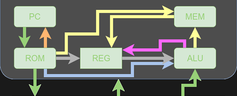
You’ll want to refer to the previous post if you didn’t read it already. The diagrams and tables give a high-level overview that will help you understand the files discussed in this post.
If you wanted to actually program this on a real FPGA, you’d have a little work to do. The memory and register initialization is done in a way that works fine for simulation, but wouldn’t work on a real FPGA. Anyway, let’s get started!
File-by-File
If you take each file individually, none of them are very difficult to understand. Here’s a quick rundown (I’m using the file names I’ll use in my online simulation):
- Parameter.v – This is like an include file that sets some basic definitions for every other file.
- prog.v – This is the instruction memory. A simple module, it takes an address and presents data for that address. The $readmemb directive reads the data from a file (test.prog).
- register.v – The register file. This is almost like the instruction memory but it has two read ports and you can write to it.
- data.v – The RAM memory. This is nearly like the registers, but larger and with a single read port. There is some simulation code that opens a file and prints the memory comments, but I deleted that as it was just for debugging. The initial content comes from the test.data file.
- alu.v – You’d think this would be complicated, but it isn’t. It just takes two inputs and does something to create the output. Something simple like adds or subtracts. The always @(*) tells Verilog not to create clocked logic for this. It just turns into some simple gates and muxes.
- Datapath_Unit.v – This is one of the more complex files, although if you dig into it, you’ll see it is mostly bulk. This file creates all the resources (like the registers and memories) and wires them together.
- Control_Unit.v – Another longer module, this one simply implements the instruction table, setting the control lines based on the current instruction.
- ALUControl.v – This file decodes instructions for the ALU. It was missing on the original post. Oddly, there is another similar CPU on the same site that has an ALUControl file, but it is clearly for a different instruction set. However, starting with that file and using the design table, I was able to recreate it. If [fpga4students] corrects this, the files may look very different.
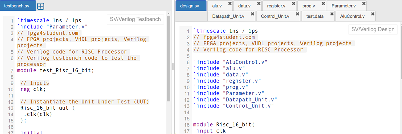
- design.sv – This file is required for the EDAPlayground simulator I’m using. It contains the top-level components (the data path and the control unit). Because EDAPlayground only processes this file, it is necessary for it to include the other files mentioned above. This causes some warnings since each of them has a timescale directive, but this is harmless.
- testbench.sv – The testbench isn’t part of the real design, but simply sets up the simulation and collects results. I had to modify it a bit to work with EDAPlayground, but the operation is the same. It just creates a CPU, feeds it a clock, and lets it run for a while. The test program and memory contents are in test.prog and test.data.
Simulation
You can do one of two things. You can open up my copy of the design ready-to-go, but that might not be your best option. I’d suggest you simply go to EDAPlayground and create a new Verilog project. Then start moving the files over from the original post. You’ll run into errors and missing files. See how many you can fix. If you get stumped, then you can use my copy to help you if you get stumped. You’ll learn more that way.
If you do decide to try it, here are a few tips about EDAPlayground. You don’t need UVM/OVM selected, nor do you need any other libraries. I used Icarus Verilog 0.9.7, but you could probably use any of the Verilog tools available. You do want to check the EPWave checkbox and you’ll need to add this to the inital part of testbench:
initial
begin
$dumpfile("dump.vcd");
$dumpvars;
Use the + sign next to the file name tabs to make new files. EDAPlayground has a limit of ten files per pane. Remember, you’ll have to include any .v files you create in either testbench.sv or design.sv. You don’t need to include the data files since the other files use them indirectly.
Run!
Once you have all the errors worked out, you can press Run and you’ll get the waveform viewer, EPWave. You have to add signals of interest so you can watch the CPU at work. It would be fun to add some I/O devices in memory or some debugging ports so you could watch things a little better. I’ll usually watch the program counter and the register write port to get an idea of what’s going on inside.
The original code had a program that exercised a lot of instructions. I commented it out and replaced it with this:
0000_0100_0000_0000 // 0000: Load R0 <- Mem(R2+ 0) since R2=0 this puts 1 in R0
0000_0100_0100_0000 // 0002: Load the same in R1 (R1 will always contain 1)
// location 8 (byte), 4 (word):
0010_0000_0101_0000 // 0004: R2= R0+ R1
0001_0010_1000_0000 // 0006: Mem[R1]=R2 (that is Mem[1]=R2
0000_0010_0000_0000 // 0008: R0=Mem[R1]
1101_0000_0000_0011 // 000A: Jump to location #4 (CPU will multiply by 2 and add 2)
// no instruction at 000C, but PC will hang there while it processes jump
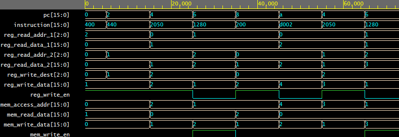
You should be able to follow the incrementing value writing to memory and watch the program counter cycle back to location 4 through each loop. Here’s a typical session:
I left out a lot of internal signals, but you can see that memory address 1 is set to 2 and then to 3 on the first two iterations of the loop.
End Game
Is this a good educational CPU? I’m not sure. Some simpler CPUs exist, but they are often small because they are tricky or they are highly impractical. Anything more complicated than this is probably too much to bite off for a beginner. While I think you should have some grasp of basic Verilog before you tackle something like this, the documentation was a little sparse (and confusing) in some areas. Obviously, it was good enough because I got it working, but if you are just starting out, you probably would appreciate a little more help and explanations.
Do you have a favorite educational Verilog CPU? I’m still looking for that one that is “just right.”


Great job ! (again)
Here is my FPGA CPU, it’s quite compact, but reasonably powerful. No interrupt support though, and no user visible stack.
https://github.com/Arlet/x18-32
Nice! Have you thought about including the testbench on GitHub?
Sorry, but I never had a proper testbench. Most of the testing can be done with the source file itself. I just had one source file with input code, and then edited that for various tests.
Where is “code.v” file? Can you give it for us? Thanks
“If you wanted to actually program this on a real FPGA, you’d have a little work to do. The memory and register initialization is done in a way that works fine for simulation, but wouldn’t work on a real FPGA.”
The initialization code looks fine to me. Why do you think that?
This is a full CPU in around 60 lines of code, both in Verilog and VHDL.
https://github.com/cpldcpu/MCPU
I have played with that one but the isa is tough on students in my opinion. At least if it is the one I’m thinking of.
Hi cpldcpu,
I can see why Al says your ISA is “rough”, however, I found your “minimal” CPU very instructive. Certainly minimal, but similar to a conventional CPU (vs one-instruction computers or tagged-transfer architectures).
With a macro assembler (like SMAL32 that you used) the extremely minimal instruction set becomes much more workable.
Of course it is a lot of fun to try and extend your minimal CPU too. I found the work of John Kent (http://www.pldworld.com/_hdl/2/_ip/jekent/FPGA.htm#Section5.3) useful in that regard.
FPGAs (or CPLDs) are great for playing around with CPU designs. Thanks for your contribution!
-Xark
Love your minimal CPU, cpldcpu. We had a challenge recently on anycpu.org to make CPUs in one page, and there’s a small but growing family here:
https://revaldinho.github.io/opc/
The first couple are small enough to fit in a CPLD. In all cases, the HDL, the spec, the emulators and the macro-assembler(*) each fit in one page – one 66-line page of green bar paper! (Emulators both in python and in JavaScript)
(*) Agreed, Xark, when you have a minimal instruction set, a macro assembler is a big win
I created a version (could be better) of the SAP-1 CPU in Veriog (I did wonder off and add a separate address bus though): https://github.com/ellisgl/sap-1-v2-mojo – It works, but there is some weirdness with HALT.
And an HTML/JS version here: https://github.com/ellisgl/SAP-1-CPU
If the goal is to use the CPU for educational purposes, wouldn’t it be better to force the student to actually build the circuits in verilog? For example, just look at alu.v. It simply says ‘result = a+b’ etc. It does not force the student to actually build the adder. So I guess the verilog compiler is recognizing what kind of circuit is required for this operation and making sure you end up with half/full adders programmed in the FPGA. It seems to defeat the educational purpose because the student is not actually building the circuits.
On a related question: If you decide to write alu.v such that you actually build the required circuits using the fundamental gates, would that be considered bad verilog code? I assume when alu.v is written as it is in this project, it is giving the verilog compiler more free rein when it comes to optimizations. Maybe specifying all the gates and building the actual circuit would end up limiting what the compiler can do and result in worse FPGA code.
I think it would be good to explain how an adder works in terms of gates, then explain how an adder works inside an FPGA, and then move on to the “+” operator. There’s no sense in spending too much time on the low level stuff if people aren’t going to use it later anyway.
The FPGA fabric has special resources for building an adder. Using the “+” operator is the best way to guarantee that your intentions are interpreted correctly, and that those special resources will be used.
Rewriting the adder in elementary gates has the risk that the synthesizer will map your logic to regular LUTs, at a significant penalty in area and speed.
The thing is, there is no single adder design – there are multiple topologies, each with their own area/performance/power tradeoff. A behavioral description will just hide all of this complexity, and your synthesis tool will simply transform it into an all-around “best guess” of the functionality that you wanted to implement.
On the other hand, if you want more control over what ends up being synthesized, then you can go from “result=a+b” to an RT-level description.
Both solutions have their relative merits, and both can be suitable for learning purposes, depending on what level of detail the learner is comfortable with – you could draw a parallel with software development, between using a high-level language and using assembly, or a library vs rolling your own.
Well, if you’re looking to improve the performance of the standard adder on an FPGA, you need very specific knowledge on that particular FPGA, and most likely you wouldn’t use RT-level descriptions, but rather open up the logic block in the FPGA editor, and map everything by hand. For educational purposes that wouldn’t be very useful, because that kind of knowledge will be outdated in a few years, as both tools and devices go through development.
I wasn’t talking about improving the gate-level description of whatever adder gets inferred by your synthesis tool (which indeed depends on your FPGA); I was rather talking about improved topologies/architectures, so not something that requires internal knowledge of your FPGA (in fact, it applies even better to an ASIC-oriented flow). Like for example going from a basic ripple-carry adder to a carry-lookahead adder, or adding Booth encoding to a multiplier – this is an aspect that you completely miss out on by writing a behavioral a+b and letting the synthesis tool do its thing.
“Like for example going from a basic ripple-carry adder to a carry-lookahead adder”
Nice idea, except the dedicated ripple carry hardware is faster than a carry lookahead using generic resources. Maybe, if you’re really clever, you can come up with a different idea, but that still requires much more specific FPGA knowledge than general knowledge about how to implement adders at the gate level. Similarly, on modern FPGAs you’ll find that the built-in multiplier is much faster than your manually encoded Booth multiplier.
“it applies even better to an ASIC-oriented flow”
Not really, because the synthesis tools know what you want (perform an addition within the timing constraints), so they can grab the appropriate N-bit wide optimized adder from the library.
So the catch-all answer here is “the synthesizer will be smarter than a beginner, so no point in the beginner trying to understand the difference between an RCA and a CSA”. That’s, you know… the best way to let him be a beginner forever.
The point here is not to cling to single examples and dispute them one by one (with a kind of hand-wavy argument, but still). The point is to recognize there are patterns and concepts that are worth learning in hardware design, and by completely ignoring architectural optimization a beginner misses out on a lot of them. Do you agree that a CSA will have a shorter combinational delay than an RCA? Then there’s something to learn from that – something that can be transferred to any RTL you might want to write, not just adders.
Saying that the synthesizer will do better is just magical thinking – there are perfectly normal people behind that synthesizer who followed the exact same path to become good at what they do.
(Meh, of course I still meant carry lookahead adder, not carry-save)
“Saying that the synthesizer will do better is just magical thinking”
That’s not what I’m saying. It’s certainly possible to be cleverer than the synthesizer, but that topic is not really good for a general education on logic design, because it’s very specific to either FPGA to ASIC technologies. For a general logic design education, I think it’s good to understand how adders (for instance) are implemented in various technologies, and then after that just use the “+” operator to get things done.
” Do you agree that a CLA will have a shorter combinational delay than an RCA?”
I agree that it requires fewer logic levels, but only if you can have arbitrary wide gates, which FPGAs don’t have.
Just to add to the lengthy conversation up there, your other question went unanswered: I wouldn’t go for writing code at gate-level, because even without getting into the performance/optmization argument it would be much harder to debug and maintain (which is where most of the time already goes when developing a product). I know of some old-school designers who used to only write gate-level descriptions, and the people I know who inherited their code are less than thrilled about it ;)
seems like that would depend on what you’re teaching them. when i took a digital logic class, we talked about adders, and didn’t talk about CPUs.
when i took a computer architecture class, the ALU was a black box that even did floating point. but we cared a lot about the pipeline, out of order execution, branch prediction and cache handling. if that’s what you’re studying, making folks implement their adders is just goofy.
nothing great at all about the promoted crippleware site. they don’t even allow normal people to register, and registering is such a pain with these clowns. Advice: don’t waste your time with EDA playground wasteware.
Hey, can someone help me perform synthesis to this design?