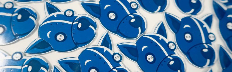
Last month I had the pleasure of creating a new piece of hardware for Tindie. [Jasmine], the queen bee of Tindie, and I designed, developed, and kitted three hundred Tindie badges in ten days leading up to DEF CON. The badges were a complete success, they introduced soldering to a lot of people, and were loved by all.
This badge was such a rousing success, it’s now official Tindie swag. We’ll be handing out a few of these blinky badges at upcoming events. But as of right now we’ve already handed out our entire stock, that means we need to build more. The second run meant ordering a thousand PCBs.
We could just do another run, and order a few more PCBs from the Gerbers I’ve already designed. I’m not really happy with the first version of this badge, though, and this is an opportunity to improve my design. This also gives me an opportunity to demonstrate my workflow for creating artistic boards in Eagle.
Effectively, what I’ll be demonstrating here is the creation of the Benchoff Nickel. A few months ago, [Andrew Sowa] took a portrait of yours truly, changed the colors to what is available on a normal OSHPark PCB, and turned that into different layers in KiCad. There are a few differences here. Firstly, I’ll be using a blue solder mask, although the same technique can be applied to green, red, yellow, white, or black soldermask. Secondly, this is Eagle, and I’m going to do the majority of the work with a BMP import. This is the fast and easy way to do things; if you want a KiCad tutorial, check out [Andrew]’s work, or my overly-involved multiple silkscreen process for KiCad. I don’t recommend this overly-involved process if you can help it. It took 20 hours to do the art for my previous project in KiCad, and I estimate it would have taken two in Eagle.
With that said, here’s the easy, cheap, and fast way of doing artistic boards in Eagle.
The Circuit
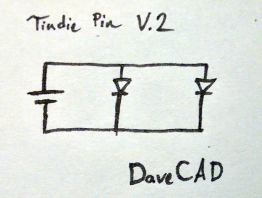 The original version of this pin featured an extremely simple circuit. The only electronic elements on this badge are a 1220-sized 3V battery, two 5mm LEDs, and nothing else. The LEDs are a bit strange — they’re low-profile, fast flicker red green and blue LEDs. They’re actually really cheap on AliExpress, they work well with the design, and experience tells me I don’t need a resistor for the LEDs.
The requisite resistor for the LEDs was a point of contention in the original design of the badge. Yes, best practice tells me I need a current limiting resistor on these LEDs. However, the battery has an internal resistance, and the LEDs themselves are more than just a semiconductor — there’s blinky circuitry in there. I doubt I actually need a current limiting resistor, but honestly, I don’t care enough to measure the LEDs and find out if I actually do. In any event, a resistor is another component in what is meant to be a kit for people soldering for the first time in their lives. There’s no need to complicate this any further.
The circuit will remain the same.
Putting the ‘A’ in STEAM
The high-level how-to for creating art in Eagle is a lot like creating artistic PCBs in any other piece of software:
- Do art. Create an image of what you want the PCB to look like. It’s helpful if the art uses the same colors as the PCB (bare fiberglass, copper, soldermask and silkscreen colors).
- Split that art up into layers, with each layer consisting of only one color. We’re basically doing a spot process here. Bonus points for creating a vector outline of the board.
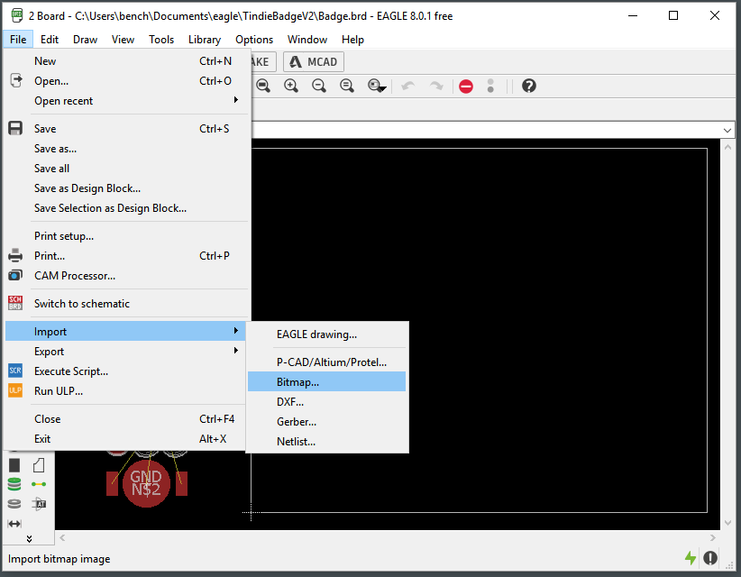
- Import the outline of the board into Eagle. Alternatively, import a bitmap of the entire image and trace around the board with a milling line.
- For each layer of the board, import a BMP into Eagle.
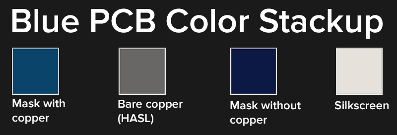
Basically, this process relies heavily on Eagle’s ability to import bitmap files. There are better ways to do this including an SVG import, but this is the fast, easy, and foolproof way. With that said, let’s continue with the working example. Below are a few swatches showing what colors are available in a blue PCB from any random Chinese board house:
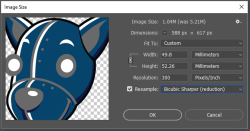
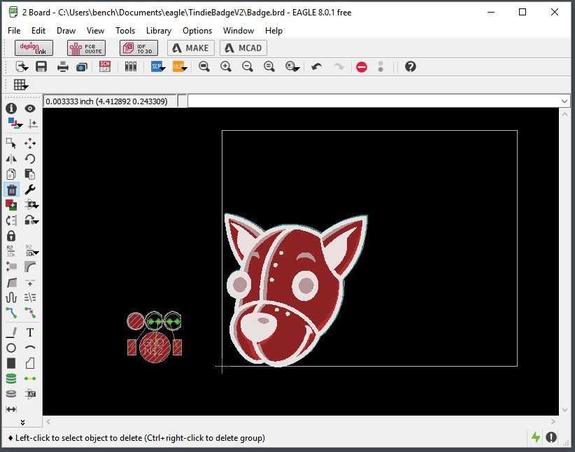
From here, it’s just a matter of taking the vector art of the Tindie head and changing the colors around. From there, it’s simply a matter of bringing this vector art over to Photoshop or your raster editor of choice, adjusting the size of the art to the size of the final PCB, and bumping the resolution up to 300 pixels per inch.


With that, we’re ready to start creating bitmaps to import into Eagle. To do that, we need to understand layers in Eagle, and how those layers are turned into a PCB.
Layers in Eagle
This tutorial assumes a working knowledge of Eagle. If you’re reading this, you’ve probably already made a board with Eagle, and you’ve ordered those boards from OSHPark or Seeed or Elecrow. If not, read this. You already know how copper, soldermask, and silkscreen works. Eagle has more layers than that; we’ll also need to work with negative layers. That is, telling Eagle where we don’t want copper or soldermask.
Here’s OSHPark’s explanation of how layers in Eagle work. Basically, we need to look at two layers. The tStop and bStop are where the soldermask shouldn’t go. This means the resulting color will be silver (if we’re using an HASL process) or gold (if we’re using ENIG process). The tRestrict and bRestrict are where copper shouldn’t go. This means the soldermask will be darker. If we were to combine tStop and tRestrict, we would get a yellow or white color — the color of bare fiberglass.
Of special note is the relationship between silkscreen (the white) and soldermask (blue, or purple, or green). Silkscreen must go on top of soldermask. Silkscreen doesn’t stick to bare copper, and the board house will probably remove it if it’s on bare fiberglass. All silkscreen must have soldermask underneath it.
Importing Multiple Images to Eagle
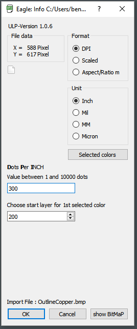
It’s time to split our art up into a handful of bitmaps and import them into Eagle. Each image you plan to import needs to be saved as a 1-bit BMP at 300 DPI.
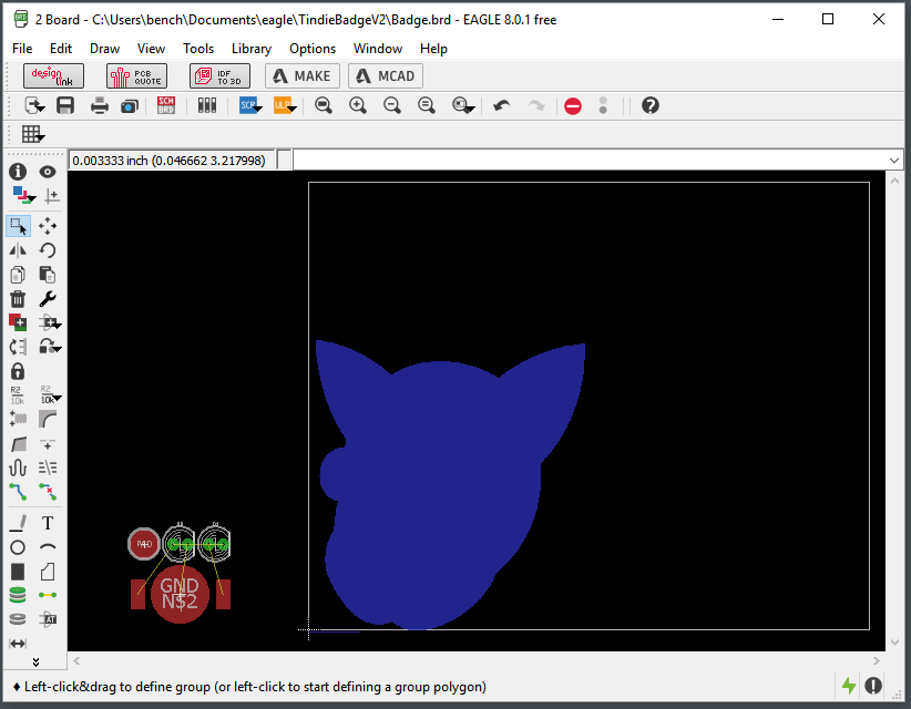
The first will be a silhouette of the entire board. This will be the top copper layer and what we’ll use it to trace the outline of the board. Yes, we could take the vector art and use a DXF import for the milling layer, but I distrust DXF imports from Illustrator, and this is a small board, anyway; doing it manually won’t take much time. Import the silhouette like so:
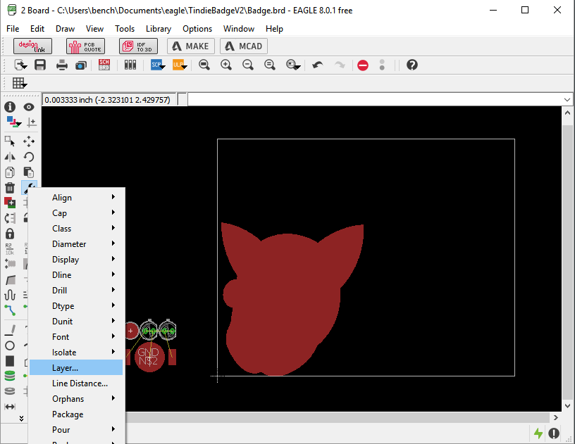
Now, we can continue creating the silkscreen, tRestrict, and tStop layers. If you’re using Photoshop or Gimp, this is as simple as selecting the relevant areas with the magic wand, and creating a new bitmap file. Take a few moments to study and understand how the images below will transfer to what we want on the PCB layers. Understanding this intuitively opens you up to a new level of artistry when designing board. Why would you ever again make boring boards when a bit of effort will produce something quite beautiful.


Since all the images are the same size, and have been saved as a 1-bit BMP at 300 DPI, importing them into Eagle automatically aligns them on top of each other. The result is a Tindie badge that should look like what we’ve designed in Photoshop:

From here, it’s just a simple matter of placing components and drawing traces. Like the last revision of this badge, I used copper fills instead of traces, but otherwise, this badge is identical.
This is the easy and fast way of doing art in Eagle. There are better ways of doing art in Eagle, namely importing areas as DXFs and manually tracing them as area polygons. In fact, this is basically what I did when I created the MrRobotBadge. If you’d like a good guide on how to do that in KiCad, check out this tutorial. It relies entirely on DXF imports, but it did take about 20 hours to transfer that relatively simple work of art into KiCad. DXF importing is a massive amount of work, but in some cases the results are worth it — I’ve been told by people who know their stuff that the mask and silkscreen work on the MrRobotBadge is the cleanest they’ve ever seen, and that used Seeed for a board house.
This is, effectively, the current state of the art in PCB art. anything with a more interesting design is entirely up to the implementation, and there are certainly artists out there more capable than myself. If you’d like some inspiration for what can be done in the medium of PCBs, there’s a Facebook group. A few people are messing around with halftone processes to get even more shades, and soon I’ll be experimenting with more colors than are available in the usual layer stack up. Until those experiments begin to bear fruit, this is the easiest and best way to make artistic boards in Eagle.


After I learned how to import SVGs in EAGLE I don’t think I’ll be going back to BMP import. Vectors just look so much better.
Sparkfun has a guide for how to do SVG import: https://learn.sparkfun.com/tutorials/importing-custom-images-into-eagle/method-1-svg-to-polygon
I see people get anoyed by this: “Putting the ‘A’ in STEAM” (I dont know what is it, not american) and you still put it in every post, why?
I see, you are the guy who turns a perfectly fine gathering into a riot, just because that will draw bigger crowds.
But yeah, if Hackaday’s goal is to maximize clicks no matter what, flame wars are your ticket. But don’t be surprised when your audience changes from hands-on geeks to hordes of rabid rolls.
trolls… damn it, I need a new keyboard.
okay okay… I’ll bite
I noticed 2 things about this post. One is about annoying people, in order to do so perfectly, always include a 10MByte (minimum size) of animated GIF, which was perfectly possible to demonstrate the blinking of the badges eyes (which we now need to miss). (fortunately there is video on the project page ( https://hackaday.io/project/26056-tindie-blinky-led-badge-v1 ))
Secondly, as the author stated “In any event, a resistor is another component in what is meant to be a kit for people soldering for the first time in their lives. There’s no need to complicate this any further.” Ahum… if this badge is to be educational should then not at least be the schematic correct, but I’ll give you the benefit of the doubt and just assume that this is caused by a bug in “DaveCAD”. The problem is that the LED’s are drawn as normal diodes, which is not the proper symbol for an LED (by the way this LED isn’t even a normal LED but a normal LED in the schematic will do to prevent things from being overly complicated, so just call this “high end circuit” an LED. Anyway, the “DaveCAD” schematic might lead to confusion for all people who are really interested in learning electronics from this badge (sarcasm may be applied) in order to learn something from it.
I can’t believe you didn’t mention the missing junction dots. Oh, how I loathe schematics without junction dots. They make my brain sore.
“People generally prefer political posts, or other inflammatory dreck.” is this an assumption? or do you have the stats to back it up?
just curious how you define and figure out what people want, what is your metric? unique page views? comments? how do you go about quantifying what people want? because from the way that you wrote that comment it seems as if you measure popularity by heavily weighting the number of comments versus other statistics.
anyways, maybe the reason you find that there is less interest in the tutorial type articles because you are really only getting the people who are into that field? i mean if someone comes here for the 3d printing content then of course they wont be interested in pcb art but will show interest in other general type posts. Posting things that are going to inflame the people who are already reading these posts may not be the best idea, especially if you are trying to increase your reader base. But then again, neither is having a writer who actively admits to and gains pleasure from being a troll.
Are you a deliberate troll or simply “retarded”? Is there a difference between art and Art, and what has doing color separations got to do with either when it is really just a simple *prepress* workflow step? You have never had a real job in industry have you Brian? I’d like an honest and open answer to my questions please, don’t try being “smart” because we can already see that you aren’t and just trying to avoid the truth makes you look pathetic.
The A in STEAM would surely require some level of creAtivity rather than just a simple technique that can be automated with a script?
STEM == Science, Technology, Engineering, and Mathematics
STEAM == that, plus ‘Art’
In America, “getting kids and young adults into STEM” was a thing. Then later, someone decided that art needed to be added to that list, for some reason.
Thanks for posting this, Brian. PCB art is a ton of fun and more people should do it!
Instructions unclear. I now have copper clad stuck in my HP Laser III. What’s the PCL for reversing the printer to spit it out?
But really: This article (and the Kicad one) are great descriptions of how to do multi-layer PCB art. Thanks Brian!
Where’s the tutorial on how to upgrade your brain to be artistic? I think I need that tutorial more :(
The crafts-person is anally-retentive whereas the “Artist” is anally-expulsive, so be careful what you wish for…
You can (for most board houses) get another color easily by using the solderpaste layers (tPaste/boasts in EAGLE). The main restriction being you can’t have silver (solder) and bare copper areas on the same copper pour touching (they would need some soldermask in between) to prevent the paste flowing where you don’t want it.
This is a great and very timely article – tho I feel like I read it long before yesterday. In any case, one area I found to be lacking for eagle was how to make a custom size PCB’s. From an image, svg’s don’t seem to convert cleanly into Eagle, and bitmaps don’t seem to work well on layer 20. instead of trying to learn yet another CAD system, After about 3 days of searching, testing and playing, I made the following gist that covers the steps I found to work well each time for making a clean DXF from an image file to import into Eagle. I made it a gist for easy access. enjoy!
https://gist.github.com/ElJefeDSecurIT/bc5015784e9dd0093efd1a859ad81ad0
For those using the FOSS PCB layout software PCB-RND, we’ve got it covered….
https://4.bp.blogspot.com/-6Ffi9OGGFnY/WbJunPBDd7I/AAAAAAAABB0/sK8MtByUrnAqtojNRPzul4ntYdyfuua2gCLcBGAs/s1600/multiple-layer-hpgl-artwork-imported-into-various-pcb-rnd-layers.png
So importing the outline (solid black) as layer 20 allowed pcb shops to cut the outline perfectly? When I created a curved outline using a line as a bmp and submitted to a DFM check it reads my outline (on layer 20) as silkscreens. What needs to be done? There are no open areas on the outline and it imports great.