If you are trying to learn about FPGAs, there is only so far you can go with the usual blinking lights and VGA outputs. Eventually, you want to do something more. Although not terribly cheap, you can get FPGA boards in a PCIe form-factor and use them directly with PC software. Is it easy? Well, it isn’t flashing an LED, but there are tools to help. [Angelos Kyriakos] did a Master’s thesis on the very subject and used a project known as RIFFA to help with the task.
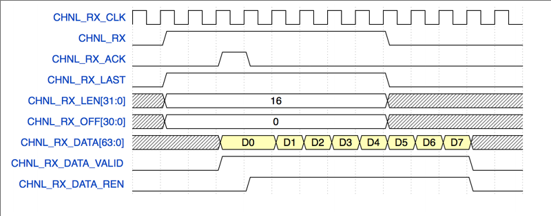
RIFFA (Reusable Integration Framework for FPGA Accelerators) is a simple framework for communicating data from a host CPU to an FPGA via a PCI Express bus. The framework requires a PCIe enabled workstation and an FPGA on a board with a PCIe connector. RIFFA supports Windows and Linux, Altera and Xilinx, with bindings for C/C++, Python, MATLAB, and Java. With proper design, RIFFA can transfer quite a bit of data in a short period of time between your computer and your FPGA.
Of course, the catch is finding a proper FPGA board, and these are not cheap. Also, RIFFA relies on the vendor’s PCIe endpoint block. In some cases, these are licensed with the development tool but in other cases, you’ll have to pay for that, too, so be sure you understand the situation with the FPGA and board you select.
Of course, RIFFA isn’t the only option. There are several PCIe cores on OpenCores, although your mileage may vary on what hardware support or how general-purpose or complete they are.
You can only hope the cost of hardware will come down. Right now the examples for RIFFA use a Xilinx board that goes for about $2,000. Numato has some boards in the $300-500 range. This board looks promising, although they don’t seem to be readily available in the United States, as far as we can tell. Speaking of outside the United States, there’s always Raggedstone. However, none of these boards are in the under $100 range, so be prepared to shell out some money.
Don’t let this put you off though. We’ve talked before about how you can do a lot with FPGAs with very little investment. Besides, you can talk to a PC without using the PCIe interface. Use serial, or Ethernet, or even SPI. It might not have the bandwidth, but it will be a lot cheaper.


If these become more affordable, the first thing I would make would be an infiniband-like cluster fabric.
Considering there are PCIe bridge chips it shouldn’t cost that much.
The Xilinx Zynq 7 XC7Z012S is quite cheap and contains a PCIe hardcore that can work in either RC or EP mode, with up to four lanes of Gen 2 PCIe.
I can’t tell you how cheap, because Xilinx chip pricing is negotiated per customer and is under NDA.
The Digikey price is too high by a factor of “several”.
Incidentally, the XC7Z012S is the same die as the larger (and more expensive, but still cheap-ish) XC7Z015 device. I believe the parts are only distinguished by efuses blown at the factory, and the development software places limits on the utilisation achievable in the “smaller” part.
You are smoking something good if you think parts with different gate densities are just software fuse limited.
Also most FPGA tools delimit free versions from those that require a paid license based on whether the parts contain high speed serdes transceivers. This usually puts PCIe out of the hobbyist budget.
They’re probably the same die, just with the subsections that don’t meet spec fused out. Whether that’s software managed or hardware managed, there’s no reason they wouldn’t as it gives them better salable yield from their fab line.
The entire programmable FPGA fabric “PL” section meets spec. and the user has the ability to place logic anywhere. The (approx.) 70% utilisation ceiling is purely a software limitation. I believe that there is nothing on the die to enforce this limitation, but I have not done any experiments (e.g. by loading an ‘015 bitstream with modified headers into a ‘012S part). I haven’t read the fine print, but I suspect this would violate the terms of use.
They do fuse out one of the two ARM cores though – the ‘S’ suffix means that it’s a single core ARM vs the dual core version without the ‘S’ suffix. Given that this is a mature process (3 gens old now), I suspect this is more to do with either reducing the die testing costs, or providing a product differentiator rather than anything yield related.
As an aside, in the Ultrascale family, the XCVU5P and XCVU7P parts have identical pairs of die, each die being a ‘VU3P part. The ‘VU9P has three of the VU3P die.
So confident… yet so wrong. Just look at the configuration user guide for the Artix-7. Same number of configuration bits means same die.
The free Vivado Webpack version supports numerous devices with both high-speed serial transceivers and integrated PCIe cores.
Xilinx webpack is free of charge for every Artix7 based chip. The pcie subsystem for DMA ip-core too. If someone is familiar with AXI4 it is a very good choice.
mesanet sells fairly inexpensive FPGA boards which see significant use by the LinuxCNC community.
the motion control HDL is open source, presumably you could cram whatever else you want on there, but i haven’t stopped to try and figure out if any of it would be very interesting.
It’s not super difficult; it’s just relatively expensive for a hobbyist. For example the Xilinx AC701 Artix 7 eval kit is US$1295. Fortunately it comes with a node-locked and device-locked Vivado license so you don’t need to have a full Vivado seat to use the kit. Most of the Xilinx 7, US, US+ FPGAs have sections of the die dedicated to PCIe and the Vivado IP catalog contains enough glue and example designs to connect the PCIe core to your logic using DMA or a register-based interface.
The trickiest bit is getting configuration completed in < 120ms so that the PCIe core is configured before the PC’s BIOS/EFI PCIe enumeration process begins. Fortunately, Xilinx’s FPGAs support tandem configuration which allows the PCIe core to be configured and start running before the rest of the FPGA is configured. The next trickiest bit is writing a Linux or Windows device driver.
As a side note, I would not recommend any hobbyist ever use an FPGA not supported by the most recent version of the vendor’s tool set, i.e., don’t buy a board with a Spartan 6 on it. ISE is an exercise in frustration.
Trying to post this for the 2nd time…
A workaround for having the FPGA come up fast enough is to add a capacitor across the reset header of the PC to delay bootup. Actually seen that used at a previous job, prior to the capacitor being added, the operators were just instructed to hold the reset button for a second or so if they had to cold boot the machine.
I found the table I was looking for in Xilinx’s DS180 PDF. The XC7A35T used on Digilent’s $99 Arty board has an x4 Gen2 PCIe core. Someone with mad board design and manufacturing skills could probably put together a board with a PCIe core using this part or one slightly bigger in the $100 to $300 price range if sufficiently motivated.
I’m interested in using a pcie FPGA card to run an online MMO server for a defunct game. It’s it even reasonable that I could use the FPGA to handle the entire server? Loot generator, monster generator and combat math… PS. The game is groom 1999, so not super hard oon modern equipment.
I hate auto correct Swype…
no
Given a reasonable enough FPGA kit, you could run just about anything. Unless you know your application _really_ well and have extreme performance needs, the usual way to approach this is to deploy a softcore and run the server on that. Then profile the application and find performance bottlenecks you can address with external accelerators and/or custom instructions. Fx. Arrow had a dev kit for which one custom NIOS II instruction accelerated a software MP3 decoder by a large factor. Another common example is an network appliance with crypto accelerators. It’s great fun, but rarely the most cost effective approach.
I wish ZTEX would come up with a PCI-E base board for their FPGA boards. I once e-mailed them the suggestion but they didn’t seem to care. To me it sounds like a no-brainer. The PCI-E block is already in the Artix-7 on those boards.
Is it a coincidence this article appeared at the same time as the one talking about desktop computers?
It sounds like a desktop on a lab bench would be the logical place to test an FPGA board, including factors like heat dissipation and RFI.
If this is leading to a PCI version of the Red Pitaya, with faster ADC’s / DAC’s – I’d be interested.
what about miniPCI?. new board with this form factor will arrive and maybe we can see cheap boards for our laptop.
I found this board for 250$. I think is the cheap and simplest option you have to evaluate PCIe
https://www.crowdsupply.com/rhs-research/picoevb
199$ https://www.crowdsupply.com/fairwaves/xtrx
Hi guys, I am interested in using the NI RIO reconfigurable card (NI 7851R contains Virtex-5 LX30 FPGA) with Matlab and not LabVIEW. All my current simulations and scripts are in Matlab, so I will be using the card as an analog data acquisition card, and process this data using Matlab on the fly. I am thinking of getting the RIFFA PCIe stack and driver and try to build them for Virtex-5 and put the final bit-stream on the card’s flash using LabVIEW. Then I use the driver and Matlab wrapper from RIFFA to read the data from the FPGA and process it using Matlab directly. I am finding it very hard to bypass NI closed box. Is this kind of logical thing to do? or am I dreaming