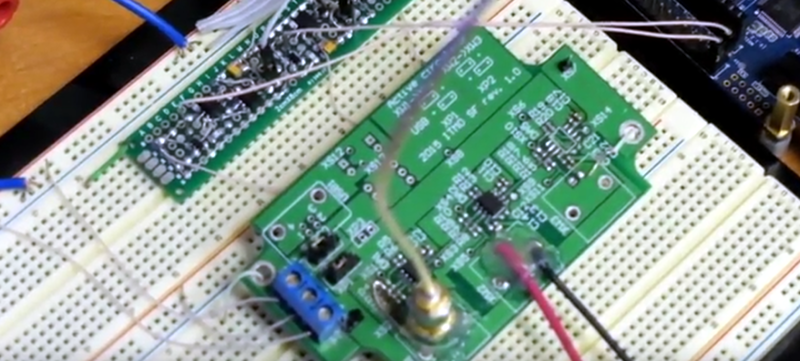
If you are working with AC circuits a vector network analyzer (VNA) is quite handy. As an entry to the InnovateFPGA competition for students, [Evgenii Vostrikov], [Danila Nikiforovskii], and [Daniil Smirnov] created a VNA using a DE10-Nano, high-speed analog to digital and digital to analog converters, and a circulator. Most of the details are in the video below, and on the project’s GitHub page.
The DE10-Nano has a dual-core ARM processor and an Altera FPGA in one package. That allows you to use the CPUs where that makes sense and still leverage the FPGA where you need high performance.
The circulator uses an op-amp to allow the test signal to route to the device under test, while steering any reflected signal back to the device for measurement. The design also uses a lock-in amplifier, something we’ve talked about a few times recently. This allows less expensive converters to generate magnitude and phase information.
Judging by the fan in the video, we suspect the setup gets a little toasty. The GitHub page has a lot of Russian on it, so we aren’t sure how much we could puzzle out since our Russian skills were mostly from watching the Adventures of Moose and Squirrel.
If you are interested in a VNA, they aren’t as expensive as they used to be. Particularly, if you roll your own and already have some things in your junk box.


Wow! (mind explodes)
A “solid state” (i.e. non-ferrite) circulator!
The only circulators I’ve seen up to this point weighed more than 100 pounds.
” our Russian skills were mostly from watching the Adventures of Moose and Squirrel.”
mine too!
B^)
The OPAMP used is pretty cool:
http://www.analog.com/media/en/technical-documentation/data-sheets/ada4817-1_4817-2.pdf
But I can’t help but wonder if a current feedback part would have better performance, or one of the new TI FDA?
I haven’t looked into this in any detail but the circulator type may be the one from https://ieeexplore.ieee.org/document/1084075/ ?
Dear James Lawson,
Our circulator was previously design for another purposes, so we just wanted to use it to increase time of development. The link you added is very interesting, thank you for your comment!
Uhh…AC circuits? I don’t believe I’ve seen a serious VNA that goes below 45 MHz. That would have to be some seriously high-frequency AC…
(Yeah, you could probably be pedantic and argue that it’s technically correct, but it just sounds silly…)
While I’m complaining, I find the use of an op-amp rather than directional couplers to be odd. I would think that the phase behavior vs. frequency would be unacceptable (or require very good calibration to compensate, at the very least).
you don’t think a directional coupler do?
I’m not sure i understand your question. But i know directional couplers are a fundamental part of any decent network analyzer. Of course they contribute to the measured signal (like any other component in the signal chain) but their behavior is simpler versus an active component like an op-amp, where you have to worry about stuff like slew rate, phase noise etc.
directional couplers have their own issues, for low frequencies opamps and resistors can be pretty much ideal
Ah I see, this is from 1khz to 50 MHz. Thanks!
Dear CE,
Previously we had some electronic devices which parameters we wanted to measure and we knew that their frequency working range was in tens of kilohertz. Of course we could use some sin generator and some oscilloscope (we actually did it first). But this project done moslty in education purposes, to show possibilities of SoC FPGA platform. The range can be increased with many known tecniques, which we can try (using frequency multipliers and other stuff).
While the results look lovely, I can’t help wondering if you could replace that DAC board with a cheap & simple AD9851 board from Ebay.
The onboard ADC is used to measure results, too. That peripheral card would be the first on the cost-cutting block.
Dear Alan,
Thank you for your comment! We actually used DAC board we had since there was not enough time to find ways to make it cheap and cool. In fact, DAC is not a good source of a harmonic signals, we have some ideas how to use meandr generator, or just implement DAC and ADC on a pin of FPGA (by using PWM and LVDS), but it makes analog part much harder and develompent time slower.
Dear Al Williams,
Thank you for this article! Our whole team was wondering how did we get so many views on YouTube, and finaly got answer)
Sorry for Russian on GitHub, but if any of readers have any questions we can answer in English! If it possible, contact me through Facebook: Daniil Smirnov https://www.facebook.com/smirnovdan
пожалуйста