
Lead-free solder alloys have been around for as long as people have done soldering, with sources dating back about 5,000 years. Most of these alloys were combinations like copper-silver or silver-gold and used with so-called hard soldering. That’s a technique still used today to join precious and semi-precious metals together. A much more recent development is that of soldering electronic components together, using ‘soft soldering’, which entails much lower temperatures.
Early soft soldering used pure tin (Sn), yet gradually alloys were sought that would fix issues like thermal cycling, shock resistance, electron migration, and the development of whiskers in tin-based alloys. While lead (Pb) managed to fill this role for most soldering applications, the phasing out of lead from products, as well as new requirements for increasingly more fine-pitched components have required the development of new solder alloys that can fill this role.
In this article we’ll be looking at the commonly used lead-free solder types for both hobby and industrial use, and the dopants that are used to improve their properties.
In the Tin of Things
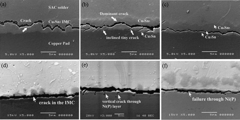
There is a good reason why tin (Sn) is so commonly used in soft solder and solder alloys: it melts at low temperatures (232°C) and offers good wetting (ability to flow on the pad) properties in addition to its ability to dissolve well with most metals. This last property is crucial in forming a good intermetallic compound (IMC). The quality of this IMC boundary determines how durable the joint will be. Both the granularity and number (and size of) any voids in the IMC will affect this durability.
The two most commonly used types of lead-free solder are SnAgCu (tin-silver-copper, also called SAC) and SnCu (tin-copper). SnAgCu alloy with 3% silver and 0.5% copper (SAC305) was initially endorsed for use in SMT assembly, along with a number of other SAC alloys. These other alloys are types with higher silver content, such as SAC387 (3.8% Ag), and SAC405 (4% Ag). These higher silver alloys are true eutectic alloys — completely changing form a solid to a liquid at the melting point of 217°C. In contrast, SAC305 has a range between 217–219°C.
Although SAC is an acceptable solder alloy, the addition of silver does raise its cost. This has driven the industry to use low-silver alloys (e.g. SAC0307) or silver-free alternatives, such as SnCuNi.
Back in the IMC
The key to a reliable joint lies in the quality of the IMC that is forced. It cannot be too thick or too granular, and preferably should not have any Kirkendall voids.
The IMC of each joint is subjected to various types of aging and damage:
- thermal cycling
- thermal shock
- drop impact
- vibration
- electromigration
Of these, thermal cycling and thermal shock are related, in that both are caused by environmental temperatures. As a joint is exposed to changing temperatures, its individual components will be subject to thermal expansion, which is likely to be dissimilar between different materials. The tensile strength of the joint then determines at which point the resulting strain will cause a crack to form.
Usually, under thermal cycling, the IMC will be subject to recrystallization, which causes a roughening of the IMC that allows for the formation of cracks. Studies have shown that adding La2O3 nanoparticles improves the thermal reliability, mostly by inhibiting the growth of the IMC. High-silver alloys also show better thermal reliability. The addition of 0.1% aluminium (Al) to low-silver alloys also had such an effect, as did the addition of Ni, Mn and Bi to SnAgCu alloys.
Drop impact and vibration are similarly related, in that some type of mechanical deformation is applied, which can affect the PCB, the joint, and the component. Especially with large pin count BGA chips, a drop impact can cause significant damage, testing properties such as the shear strength of the joints. The failure modes from mechanical vibration are similar to those from thermal cycling, caused by the gradual development of cracks.
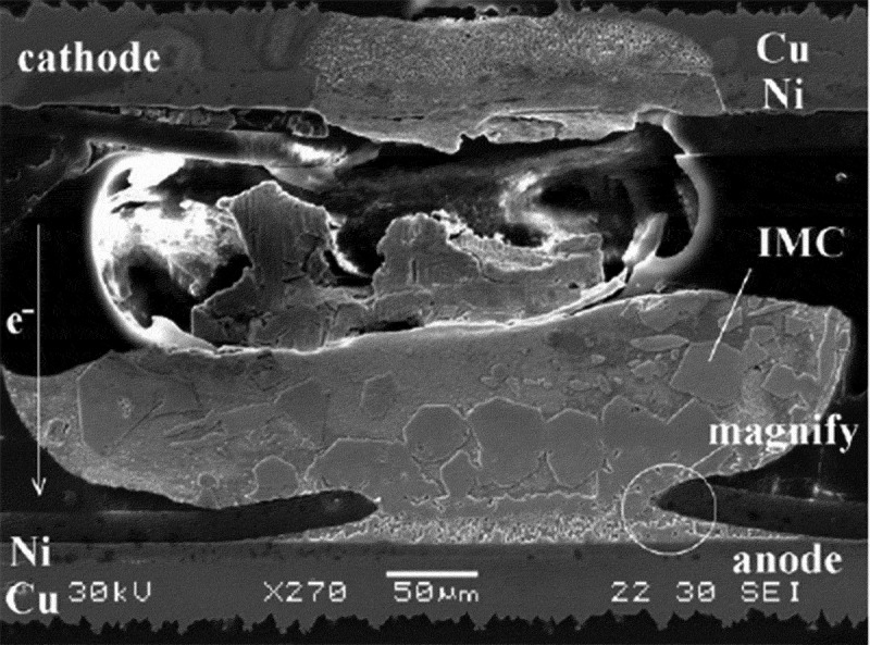
Finally, electromigration is the most insidious of all, as it does not require any external influences. The ultimate effect of electromigration is the transport of material within the joint and IMC, caused by the gradual movement of ions, as momentum is transferred by electrons and diffusing metal atoms. The current within the joint between the anode and cathode causes cavities to form. Over time, these voids become large enough that cracks can form in the joint and IMC until ultimately the joint fails. At higher temperatures and currents, this process accelerates.
Preventing electromigration involves regulating temperature and current density, as well as tweaking the composition and structure of the solder joint to increase their electromigration resistance. Adding cobolt (Co) was shown to improve electromigration resistance, as did the addition of nickel (Ni) and bismuth (Bi), with the latter also decreasing the melting point of the alloy. Both seem to improve the electromigration resistance through the inhibiting of the growth of the IMC, which appears to be a key element.
More alloy with less
During the 70s, 80s, and much of the 90s, virtually all soldering was done on relatively large pads. Most if not everything involving through-hole soldering using DIP packages or similar. As surface-mounted soldering and the use of smaller packages such as SOIC, TSSOP, QFN and BGAs became commonplace, the strength of the IMC and its durability became much more of an issue as pads became smaller and smaller.
As we saw earlier, electromigration is a major issue which along with those of thermal and mechanical resilience will play major roles now and in the future. Solutions to those issues will determine much of the lifespan of our devices, as well as whether dropping that new smartphone will be a mere annoyance, or fracture half a dozen minuscule solder balls on the main, 0.2 mm pitch BGA package.
Enter SN100C
Although SnCu as alloy is not preferred for soldering as the copper tends to form a rather coarse and brittle IMC, a micro-alloy variation on this that can compete with, or outperform SnPb and SAC alloys has been around since the 90s, when Nihon Superior developed SN100C, which is SnCuNiGe. Unfortunately, this alloy has been encumbered by patents until quite recently. It has its melting point at 227°C, with the 0.05% of Ni promoting a shiny joint while lowering copper pad erosion. The 0.009% of Ge promotes wetting and prevents the formation of dross.
With this eutectic alloy being cheaper than SnCuAg alloys, and its better properties with for example reworking, it appears to be an interesting choice for both professionals and hobbyists. With the patent having expired (yet ‘SN100C’ still trademarked), many manufacturers have now added this alloy to their catalog, including Stannol and Felder (Sn100Ni+), making it much easier to procure.
Materials Science is About Compromises
At the core of soldering alloys lies the realm of materials science, which is by definition one of compromises. Enhance one quality in one area, and degrade a quality in another. We can see this when we look at using micro-alloying to improve the mechanical stability of the IMC, resulting in worse electromigration resistance, and so on.
Sometimes the statement is made that we had found the perfect soldering alloy with 63/37 SnPb solder, but as electronics miniaturizes ever more and research on soft soldering alloys progresses, we can see a number of requirements appear that were not even remotely an issue back in the 1990s, yet where we can now apply new knowledge to solve them. Reading through scientific papers from 2005 on the topic versus today really shows how far we have come already.
One of the most annoying properties of tin — tin whiskers — still remain one of the hardest to fully solve. Although lead (Pb) did inhibit the development and growth of tin whiskers, it was not a perfect solution. Alloys like SnCuNiGe at this point appear to offer comparable performance in this regard and have been recommended as a drop-in solution.
Building a Better Alloy
With issues like the thermal cycling and shear strength of ever-shrinking solder joints becoming an issue, the refining of the alloys we use for assembling PCBs is something that is worth tackling. If we can make the assembly of 500+ lead BGA packages and their reliability over 10+ years of daily use into a near-certainty, then that means less electronic waste that needs to be recycled, or which ends up in landfills.
Similarly, having easier to use and more reliable alloys for hobbyists is also becoming more of a topic. Hobbyists are no longer merely jamming a couple of 74-series DIP ICs into a through-hole board. More often we see QFN, TSSOP, and similar packages are being used. With improved wetting and decreased bridging potential of new alloys, it should make life better for everyone.


In my opinion, the best leadfree/leadless solder is not better than the good SnPb stuff. So I stay with that for everyday lab and hobby use. Let the leadfree stuff be reserved for the industry with their well tested and optimized manufacturing processes like nitrogen flooded reflow ovens.
OK, I did not know about SnCuNiGe and it’s good properties. But there is still the melting point issue: 227°C! Thats 44° more than the 183°C of Sn/Pb. 44° which reduce your process window or increase the thermal stress on the components.
So is Sac305 equivalent to sn/bi ?
definitely not, SnBi (approx 52-48 ratio) has very low melting temp. 138 degrees C while SAC305 has 217
Agreed. And nothing else has the authentic flavor of the old sk00l stuff, either.
“Not better than the good SnPb stuff.” But how good do you really need as a hobbyist? Are you actually using those margins? I’ve never had a joint fail with leadless solder, nor have I had any trouble working with it—and I solder all the time. I think it’s fine. It’s easy to quibble about minor stats and technical variations between the two when you’re looking at the graphs and such, at electron microscope images of someone else’s failed joints, but then you distract yourself from the practical reality that they both work just fine in nearly all cases.
Plus, I think there’s a certain vein of traditionalism in engineers. Which is fine, there’s a reason for it. I like it most of the time. But occasionally it’s too stubborn and reactionary and gets in the way of practices which are just and good.
if you work with MILSPEC, it’s really hard to pass QA with leadfree circuit boards
“But how good do you really need as a hobbyist? ”
“If you work with MILSPEC it’s hard to pass QA”
I doubt there are many hobbyists who are cranking out hardware in their garage to fulfill military contracts.
Just as an example; I might be repairing or improvising field grade gear for farm use in my shop. “Military grade” doesn’t help much when the application is something like plowing drain tile. “Best I can do” is the least I want to put forth there.
Yeah it is a bit tedious but entirely pervasive attitude humans have.
No matter how hard I suck at tennis I think I need a rachet that looks like Nadals etc.
My ford focus needs fuel with an octane rating fit for a lambo.
People love to make a fuss about lead free solder but I use the stuff all the time and have never noticed the disasters people predict. Even when I was doing fine pitch soldering (modding some consoles) whenever I reviewed the work I never noticed the boogie men spindles which everyone else seems to get if they so much as solder a eBay clock kit with leadfree.
>My ford focus needs fuel with an octane rating fit for a lambo.
You wouldn’t really want an engine that didn’t. A Lada 1500 runs on 75 octane fuel – because it was designed to run on Soviet gasoline.
@Luke
Not a lambo fan?
I don’t understand your point. Modern engines are designed to use high octane “racing fuel” because they need the high compression ratios to pass the fuel economy standards. When the EPA test is over, they re-program the car with retarded ignition timing to allow them to run on regular.
“But how good do you really need as a hobbyist?”
My parents have items such as a lamp and furniture that were built by my great great grandparents over 100 years ago. They are still functional and in regular use today.
I want immortality through at least a few of the gadgets I leave behind just like they have. That’s how good I really need as a hobbyist!
> I’ve never had a joint fail with leadless solder,
I have. One board I made with a SnCuAg alloy dissapeared into white dust because of tin pest.
I think a hobbiest is MUCH more likely to take advantage than an industrial process.
At the very least, I know I end up re-working my boards infinitely more often than your typical production device.
44°C is a huge heat difference when you’re doing hot-air rework of SMD components. In contrast, there is zero advantage to switching. And the lead free alloys are more expensive. There’s nothing “just” about them either. The only reason to switch is if somebody is forcing you for non-technical reasons.
Any desire to use lead solder should be interpreted as brain damage from too much lead exposure. Sure, go ahead and make your one-off projects with lead solder, and make sure to leave lots of lead residue on your hands so your children can also enjoy the fun.
“Washing skin with standard soap and water is not enough to remove lead residues” – Centers for Disease Control
In a study published in QEX, geometric mean lead levels in keen homebrewing radio amateurs were around 2 mcg/dL, which falls pretty much within normal population levels.
People, and kids, are more likely to imbibe excess lead from shooting ranges or environmental sources such as nearby smelters, mining operations with ore crushing or from leaded paint.
And atmospheric lead from vehicle exhausts was, for most of the 20th century, the predominant way lead got into a person in most of the world. Lead exposure from home soldering is not a significant health concern – the worry is lead from electronic waste leaching into groundwater.
Metallic lead doesn’t really dissolve into water.
Lead in combination with carbon forms organic lead compounds which are the real danger because they’re fat soluble. This combination happens when you burn lead with some fuel containing carbon, like gasoline, or gunpowder.
I think I read that acidic water will carry elemental lead.
Flint MI may have something to say about that.
In Flint they changed the water source and put raw untreated water into the pipes, which started corroding the pipes.
Point being that water from a river tends to be slightly acidic. It has to be treated to neutralize it before you put it in your water supply because it would eventually destroy your pipes anyhow, lead or not. GM was using the water in their car factory and complained that it was corroding their car parts – it was that bad.
This wasn’t done in Flint because they were being cheap. They were saving $140 a day by not adding the corrosion inhibitors to the water. Lead wasn’t the only problem – they had coliform bacteria in the pipes as well because of the raw untreated supply. As a response, they dumped a whole bunch of chlorine in the pipes, which only increased the corrosion problem.
The GM plant saw corrosion because the water company was putting excess Chlorine in the water because IRON was being exposed when the anti-corrosives were eliminated. With the exposed iron, it formed ferroous (ferric?) chloride, removing the free chlorine from the water and allowing bacteria to flourish. The GM problem had nothing to do with acidic, raw, or otherwise untreated water and a lot to do with bacteria and failure to protect the iron pipes in the first place.
At no time was untreated water put into the distribution system.
“geometric mean lead levels” means that a home with one highly concentrated lead deposit will read out as “within normal population levels”.
Who are you going to trust with the health of your children? People who literally call themselves “amateurs” or the Centers for Disease Control?
“more likely” what does that mean? How do people who don’t go to a shooting range get lead from a shooting range?
Everything you say is complete nonsense because the damage is additive and cumulative, not “instead” and there is NO known safe limit, any and all exposures are bad. Your kids are going to spend a lot more.time in your house than they going to spend at a shooting range.
“Protecting children from exposure to lead is important to lifelong good health. No safe blood lead level in children has been identified. Even low levels of lead in blood have been shown to affect IQ, ability to pay attention, and academic acnievement. ” – Centers for Disease Control
Oh, no! It’s lead! Run away!
Oh yes, it’s lead. Stay away.
The effect of lead exposure on IQ test scores in children under 12 years: a systematic review and meta-analysis of case-control studies
https://systematicreviewsjournal.biomedcentral.com/articles/10.1186/s13643-022-01963-y
I’m not sure you know how lead toxicokinetics work, how epidemiological studies are undertaken, how risks are ranked, and how characterisation of means in log normally distributed data sets of small size are dealt with – all of which impact on interpretation of the results and ranking the risk of Pb/Sn soldering relative to other environmental and occupational sources.
and there’s methanol in your apples, formaldehyde in popsicle sticks, and a toxic dose of salt sitting proudly in the middle of the kitchen table.
So you’re saying that formaldehyde is safe, right? No worries? No warnings?
I think the amount of lead you would be exposed to by occasional soldering is relatively benign compared to all the other chemicals involved in PCB manufacturing and repair.
You should consider personal safety for all of the stuff you are handling.
Regarding lead, many Europeans are still drinking tap water from lead pipes. It is considered safe as long as there is no modification made to the plumbing due to a mineral crust buildup inside over time.
I hope you will have your children watching from a safe distance no matter what kind of solder you are abous to melt. Flux formulas are no less toxic.
This has gone way off topic. Sorry for that.
And leadfree solder often needs more aggressive fluxes.
> How do people who don’t go to a shooting range get lead from a shooting range?
Lead dust sticks to your clothes and on your person, and you carry it back home, slowly poisoning your children. There was also one case where the shooting range had a ventilation system blasting unfiltered air directly at a kindergarden down the street. and another case where the range workers were just sweeping the lead dust out the back door when nobody was looking, contaminating the whole neighborhood in both cases. There’s surprisingly little oversight.
the actual health risks from lead handled correctly are pretty low. Solvents and flux is a bigger health risk, All the lead weights from car wheel weights and batteries make up more lead then all electronics, and solid lead is not floating thorough the air like radiation. The down side of not using lead is pretty large, compared to the political feel good benefits. The real solution for these materials in electronics would be to handle them correctly, and recycle them when they are tossed. We have ramped up requiremts for electronic disposal and recycling, despite the RHOS dictates. On the flip side, in the interest of going “green” we allow and encourage MERCURY in glass tubes for fluorescent lighting, Not banning flourescent lights is such a glaring inconsistency, it makes it obvious how much of “green” is political, and not smart “science” or engineering.
Sounds like you are one of the leftist “SCienCE!” cult members, not a promoter of actual science. Issues with Lead are from vaporizing it, or having it in a chemical form that can turn to dust and be inhaled or eaten, such as in paint, or as mentioned in. other contents putting it in gasoline and burning it. The really dangerous stuff with electronics mfg, is the solvents. Obviously you shouldn’t eat and solder in the same place, and you shouldn’t spray paint stuff in your kitchen either, or clean plates with gasoline. The same rules that have banned lead in electronics, allow MERCURY in breakable glass tubes everywhere- fluorescent lights. Those should have been banned long ago, and especially now with LED technology, there is no excuse for them, yet there they are. If we require recycling electronics now anyway, if handled correctly lead is a huge benefit in electronics (especially aerospace and medical) and a small risk compared to many other chemicals we use. All the lead in electronics worldwide was a fairly small volume, less than lead weights on tires when they were used. Forest Mimms did an analysis of it I read at some point, interesting points.
You can have my leaded solder when you pry it from my cold, dead, diseased hands :-P
Shouldn’t be too hard to pry it off of you now considering one of the symptoms of lead poisoning in adults is joint and muscle pain. (c:
Lead poisoning symptoms in adults
I handle leaded solder my life. So do my colleagues.
No health issues.
It seems to be a common mistake, that leaded alloy harm the producers of electronics.
Normally that doesn’t happen.
There is a PD that is used to make his students calc the extra energy that is needed to solder with leadfree… “Green” isn’t so simple either
Nice n=2 data, wonder what larger scale data collection suggest? Oh wait Lead = Bad.
Personally I don’t care if you smoke ricin. But in countries like the UK with shallow water as our only water source we need to externalise anything that might reduce it’s quality.
That all this is. It’s the same as littering. You personally can always discard your Tesco bag for life into the nearest field and you will never detect any harm from it. But it is a problem if it’s something many people do.
I don’t care if they do it, but the attitude they have of wanting to teach all the newbies to do it too is awful, and is why we have to have so many manufacturing rules.
Hopefully at least some of the newbies will recognize, “oh, if I want this to be a marketable skill I should be used to the stuff that is allowed to go in products. Especially since the old timers say it is so hard to switch if you learn the wrong one.”
Nearly no series products are hand soldered any more. And for lab use ore the one-off amateur project it doesn’t make a difference for the environment. So lets use what gives the better result.
Hm- I work in the electronics production for 10 years. My ham-radio OM getting very old, too. And i never ever heard or met someone with a lead poisoning on a congress ->(n=1000). Many “safety”-products still running on leaded alloys.
Just imaging all the fishers and firearm friends handling lead pieces and bullets their whole life too.
There are no special handling or safety warnings for lead (okay… Don’t eat it, don’t drink it hot), but the flux fume is dangerous, of course.
But on smt the amount of needed alloy is so small…
Nobody could imaging how small the joins will get. Wave soldering and hand soldering as no real meaning in many new products…
But we have to dig and waste silver.
The people don’t see the big picture. Many “bad stuff” is easier to recycle or last longer.
You soon will see what happens if chrome will be forbidden. You have to paint or replace parts on and on…
And yes- burning electronics in a barrel in Africa is a bad thing and poisoning
>Nearly no series products are hand soldered any more.
Power electronics; large filter capacitors, coils, transformers, etc. are still hand-soldered in many products because their shapes and sizes make automatic assembly difficult. This often happens at the point where the product would go through QA and inspection anyways, so the guy who does the testing puts in the last few components, cleans up flux residues, and sticks it in the testing jig.
Well Luke,
Maybe we work in different markets.
All EMS I know as well as our production try to avoid every extra step (lean). Therefor all try to replace THT with SMT, use Pin-in-Paste/Paste-In-Hole even “backside reflow”.
On one congress a producer of warm water heater showed us tests, for I guess 100.000€, to find one pcb flux combination that make a BTC run on 400V and 20A with 85/85 conditions.
BTW: cleaning no-clean paste breaks up the encapsulated chemicals and raise the risk for metal migration.
Will not be able to clean under BTCs anyway
@[Daniel],
Are you saying some BitCoins (BTC) are dirty?
As in money laundering? Or leave a filthy residue where ever they have been?
@ren: abbreviations… Just 36^3 – or more realistic – 36x26x36 permutations for three digits…
Of course BTC is here Bottom Termination Components. So QFN, DFN, XDFN, LGA,….
Even surface mount components, if you have a large filter coil, you’d have to stick the board in the oven for 10 minutes before it heats up enough to flow the solder, so the component is soldered in by hand instead. This is on products like power conditioning boards for radio towers etc.
What research shows that lead in electronics is getting into water, and is a bigger problem than say mercury in fluorescent lights? “SCienCE!”
lead is a silent killer its takes many years for the effects on lead within your body to show ,best of luck
Come on.
I handle my whole life less lead than a gun man or a fisher in a year.
My parents had lead in the color of there toys. My father is now over 80.
You think in dimensions of lead water pipes or cups of lead.
But that is not what happens if you are handling with electronics.
I know some many old electrical engineers, if you were right, they all must be lead poissend.
But because of high income and good health insurance they get very cold.
You really should start reading “Factfulness” or something like that.
It’s this “you have to drink a container full of it, before it really harms you”, but next drug party, Marathon, climbing tour or even car driving has a much higher risk to take you years of your life
Yes, much like fat, cholesterol.
If you’re doing 1,000 boards/day, you shouldn’t have your people handling lead all day. Just as they shouldn’t eat chocolate all day. Or red meat for every meal.
The next time you place an order for 250 pounds of solder, it should be lead-free.
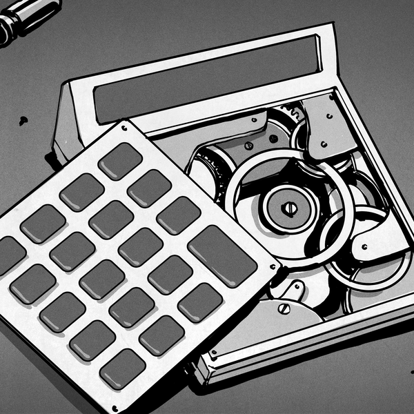
I’m finishing up a small roll of solder I bought at Radio Shack. Yes Radio Shack. Meaning that roll has lasted me at least ten years. The roll is maybe 4-8 ounces.
That’s analogous to eating a one Quarter Pounder with Cheese every ten years. The risk is so small as to be not even worth thinking about. There’s a greater risk that a spider will crawl into the roll of solder and bite me when I pick up the roll.
Considering that the symptoms of lead poisoning can include vomiting & diarrhea you can keep it.
Didn’t nobody tell you, that solder is no food?
No…no lead-free solder…..I refuse to use it!
+1
This page causes Firefox to throw up a security warning because the pciture of the roll of solder (http://hackaday.com/wp-content/uploads/2008/05/dscn1486.jpg) is linked via http not https…
While the https-always-for-all-components-of-all-sites policy is arguably overkill (wasteful of energy on both server and client side, feeding the bottom line of crypto accelerator manufacturers even for documents where there is little to be gained by encrypting them in transit or even from message authentication) it’s almost certainly intractable to try and declare a less draconian rule for when to balk at non https traffic without leaving loopholes for malicious actors…
In any case, the URL in question _does_ work via https so a single character change to the page source will fix this.
Huh, no idea why this one image got linked without https but I’ve updated and seems to satisfy the warning. Thanks!
It’s so the man in the middle can’t guess what you’re looking at by observing what content you are downloading.
Secondly, it’s so you don’t accidentally get tricked into an unsecured connection for when it does matter.
I hate Sn100% solder, but I have to use it in my workplace (SMD rework), because SnPb is forbidden.
I have been wondering which of the many “witch’s brews” of Lead Free solder would be worth obtaining,
but, in some cases, I didn’t want to spend decent money for something that had no noticeable advantage over Sn100%.
So, based on this article, I am willing buy a small spool of SnCuNiGe, and try it.
I will welcome opinions pro or con from readers.
I use Sn100Ni+ from felder, nice solder, much better than SC305 as it is eutectic, gives nice shiny blobs and good wetability for a lead free (still far from SnPb tough).
I tried to read through the whole thing but so much of this is over my head. Wish there was a tl;dr eli5 for what kind(s) of solder are the most viable replacements for solder with lead in it. People have always told me that lead-free won’t last as long but if lead is being phased out then we’ll all have to switch eventually.
I think the section you want to read is the one on SN100C.
You also might want to consider SN100E, which may be cheaper than SN100C.
The simplest thing is, if your application high current, high vibration, or runs in an environment with high temperature and high humidity, then don’t buy the cheapest Sn, buy any of the alloys that fits your price range.
Most projects and products never end up with any bad solder joints, regardless of what type you use. But if you end up with one of the problems in the article, try an alloy. The more expensive ones are better, but not needed to get a good joint.
Pure tin develops tin pest under 13 C so if you have anything that has to stay outdoors even in relatively benign environments, Sn100 or Sn99 alloys are a no-go.
Incidentally, the addition of Germanium accelerates the process, so SnCuNiGe is also terrible for any electronics you might want to leave in your car or store in your shed. These alloys are tested to stand for 6 months under cold temperatures, because the phase change reverses itself when the item is brought back to room temperature – but it also has to stay warm for months before the reverse happens, so this gradual back and forth change from a to b phase erodes the joints.
I observed this effect with some hobby projects, where I left the part in an unheated garage. After two winters, all the solder joints had turned to white dust.
Even when I did a bike light corrosion test and left it outdoors 24/7 with no coating at all on anything, just an exposed proto board with LEDs and a switch mode CC circuit, with occasional vibration from riding (mounted with zip ties) it was fine. After 3.5 years I moved and I can’t leave it outdoors anymore, ending the test. The exposed wires including LED leads are visibly corroded, but there are no problems with the solder joints.
It is only a problem in a small number of specific environments, like the Southern US, or in high current applications.
It is a real effect that exists in the world, but it is not a typical effect that is normally experienced, even with unprotected circuits. And a conformal coating reduces it substantially.
I have the following procedures:
When reflowing new boards I use SAC305 paste as I have initially adjusted the process to that alloy. Haven’t had any problems, and if you possibly want to sell a board once in a while it needs to be ROHS compliant anyway.
For hand-soldering of prototypes and repairs I have always used SnPb with great success and I am not planning to change that habit anytime soon. Why should I?
Does anyone know what alloys electric vehicles are using? Especially Tesla. High current – check. Thermal cycling – check. Thermal shock – check. Vibration – check. Cost conscious – check.
Where? – there are so many different PCBAs in a car… I’m quite sure that some high current parts even need “all most sintering” processes. Some might be so critical that the paste will contain indium or complex alloys like SnAgCuBiSbNi.
I was thinking about the high current parts, such as motor controller and battery charger.
Well – I’m working with very small components.
But I know researches from that market.
It depends on the chip they use.
There many tricks out there. Of course the have to avoid voids. So the alloy is one thing, but the flux is a bigger problem-> plasma cleaning or “ant acid” and the need vakuum-reflow.
Some add copperballs to the alloy.
A new shooting star is a special sintering process.
But as Luke already mentioned: spot welding on the batteries and aluminum bonding to chip will be the todays best practices
Thanks for the information. Very interesting stuff.
They use spot welding in the critical parts.
I’ve been using SN100C for commercial products for over 10 years. (Went straight to it from SnPb.) I agree that nothing compares to SnPb, but in the leadfree world SN100C has been a great thing for me.
TNX for the high quality cross walk through the alloy topic.
If you joining German SMT congresses, you will see a lot of researches with different alloys. But if it comes to industry products- the biggest market in Germany- the most products use SAC305, if they can.
One reason are the BGAs with their SAC305 balls. That might be an explanation why leaded alloys sometimes fail earlier in the TCT, too.
A other point is the temperature range (PSL) of the parts. Some Parts can’t take more than 240°C for a few seconds. So b.e. SN100C provides a to tight process window on a mixed sized parts designs.
Low temperature alloys on the other hand can be critical in combination with high density processors or power chips that getting very hot…
Germans, with their SAC305 balls in their big MAN diesel trucks.
Interesting article, but where is the info about those low-temperature alloys that are of special interest to hobbyists, with exotic alloys containing bismuth and/or indium? Like the “Maker Paste” sold by Adafruit…
+1
Writing about SN100 as a solution is a number of years out of date. So many other options now. And I hope no one thinks that SN100 means 100% tin, because it is not……
Sn100 has terrible wetting for hobby use! I wouldn’t use it for home use, only professional for low cost in standardized processes
OTOH if your hobby stuff is through-hole, you might not even notice the difference. They all work fine. :)
I tried a lot of different alloys since the inception of Pb-free solder. My hobbyist summary is: wetting is the problem. SnPb is much superior due to the better wetting ability. So far, no lead free solder has come close. I tried the Germanium alloys, the Bismuth alloys etc., it just doesn’t wet as well and often not properly. I can only recommend two different types: the Amasan 26 type (higher number is also ok) as well as the 3-4% Ag stuff from Almit. Gummix flux has the added benefit of not causing hot resin droplets from flying around. For the last two years I’ve been using nothing else than Almit LFM-48.
63/37 leaded solder works just fine for me. It’s easy to work with, low cost compared to many of the lead-free products, can set my iron to a lower temperature compared to lead-free prolonging tip life and reducing the risk of board damage.
lead-free solder, a solution in search of a problem.
All of this debate over “why do hobbyist need MILSPEC builds” got me thinking about why I espouse this mentality (and use Pb solder both at work and at home).
As a hobbyist (or limited use professional) I tend to have less control over the variables involved in the manufacturing process. I am far less temperature, humidity, pressure, airflow, etc. etc. controlled and risk a much wider array of contaminants that larger manufacturing facilities. Taking out one more variable (the somewhat magical failures of lead-free solder), and focusing on all of the other reasons a device might be malfunctioning can really help manage the cognitive load of creating something.
Once a project scales to a massive production process necessary changes can be made to switch to a lead-free solution in most (low-shock) applications.
This is exactly what I meant with my initial post. Also at work, for lab use (hand soldering, patching of prototypes) I use SnPb. The series production stuff is manufactured by an EMS partner anyway and he uses Pb-free.
At the end of the day:
https://nepp.nasa.gov/whisker/reference/tech_papers/2011-kostic-Pb-free.pdf
“A huge (~ $14B annual revenue) semiconductor manufacturer estimated the annual worldwide Pb reduction per 1,000,000,000 integrated circuits was only equivalent to ~100 automobile batteries–This is less than 0.05% of car batteries that are not recycled yearly”
+1
Exactly, it is completely political and has no sound objective perspective behind getting rid lead in electronics. I keep wondering how in the world fluorescent lams with mercury in a delicate glass tube gets a pass, but lead which is less dangerous that some fixes and MANY solvents if handled correctly is treated like some highly radioactive material. All political, “SCIenCE!!” not real science.
sorry about the typos!
i think lead solder is better because .
1. it has a lower melting point you dont need to turn up the heat to melt it.
2. it seems to be stronger so we did not have cracking of the connections resulting in the 2007 mac book pro gpu black screen of death gate and the xbox red ring of death gate.
the only times we would have any defects like that is if the manufacturer felt a little adventurous and decided to start putting the boards through the wave soldering machine too soon and the solder was not fully melted but would only effect the first few boards.
why it is happening now is because manufacturers are using lead free solders witch has a higher melting point they are not turning up the melting pot or getting a melting pot hot enough to handle the rohs compliant solders and maybe even running the boards through too fast.
I really feel for those that still think that lead free is challenging. I use both SN/PB and SAC305 flux cored wire solder and solder paste at home and there is only one difference between the two: the tools I use for them. I have said it many times before that the number one challenge people have with lead free is with not using the right equipment. When I hand solder with SAC305, the only difference to my methods is the tip I use in my old Metcal SP200. (different temperature). Apart from that, I solder the exact same way I solder SN/PB. Using the right equipment is literally the solution.
I work at an EMS and I keep thinking I should record one of our rework techs soldering with SN/PB and then with SAC305 to show people how similar the two techniques are when using the correct tools.
Thanks for your compassion!
“the number one challenge people have with lead free is with not using the right equipment.”
Trying to convince my employer is the big hurdle!
Read it and may I summarised – Sn100c for basic solder things’ feet into holes on pcb after breadboard work; just for self use ?
So we are all talking about soldering alloys, but nobody mentions the Bi58Sn42 alloy yet? Unlike many other lead-free alloys, it’s a true lead-free eutectic alloy, and has a melting point of only 138 °C. Although it’s primarily designed as a low-temperature alloy for heat sensitive components and desoldering, but it’s also an usable generic-purpose through-hole soldering alloy, has a reasonable strength, and it produces a brighter joint than SAC305. Wikipedia claims it’s “used extensively in through-hole technology assemblies in IBM mainframe computers where low soldering temperature was required.”
It’s not to deny its own problems. First, when it’s mixed with leaded solder, the melting point and joint strength degrades significantly (which is the same property that makes it useful for desoldering), never mix them. Second, its joint strength is reasonable, but not as strong as SAC305, and finally, its surface tension is lower that both SAC305 and Sn63PB37, which may make it difficult for manually reflowing small footprints, which heavily relies on the self-reflowing of solder under surface tension to make its connection.
But certainly, it has its use in your toolbox. I have a few rolls of Sn63PB37, SAC305 and Bi58Sn42 on my workbench. Perhaps it’s time to buy another roll of SN100C as well.
The low-temp alloys are excellent for desoldering of sensitive components, when you want to minimize their heat load. Coat the pads thickly with this and it dissolves the higher-melting-point solder.
Picquick Desoldering Alloy is something like that.
If you aren’t afraid of cadmium, Wood’s metal will do even better job. (Cadmium tends to form volatile oxides, but the soldering temperatures aren’t high enough for concern. Flame-brazing warrants precautions.)
Fear of lead is grossly overrated. I never saw any report that would hint on any significant exposure from its alloys (except in dust form).
For home use, the fumes from more aggressive fluxes, the outgassing from materials exposed to significantly higher temperatures needed and the stress on the operator from poor wetting are more health-damaging than the minuscule exposure to the solid metal surface. In long term, you can also add the stress impact from handling unexpected failures due to tin pest, cracking and tin whiskers.
For commercial use, in small handmade series the chance you’ll get caught is minimal and large series get outsourced anyway.
There are Bismuth-Tin soldering alloys with some silver in it, which improve many of it’s characteristics (Especially the brittleness). It’s straight out better than lead-tin, except for a little worse wettability, which I don’t really give half of a crap about.
And as said here https://www.bhencke.com/blog/2019/3/15/a-hill-to-die-on
People who solder with lead are exposed to lead dust daily, because you clean your soldering iron with a brass wool that literally turns the solder into dust. These people would know this if they weren’t suffering from lead poisoning and the “muh rights to ingest toxins” disease
I enjoyed working with leaded solder until my heavy metals test report arrived with toxic levels of lead. I am seeking alternatives. Thanks for the info! Good luck lead lovers! I recommend reading medical based articles related to lead toxicity.
These “new” alloys sound interesting, however, where to buy them? I don’t see any at RS or Farnell.
I came here looking for a discussion on 99.3/0.7 SnCu vs 305 SAC, but this SN100+ solder is interesting.
As someone who works with old cars, sometimes goes shooting, and has weird health problems, I am glad to eliminate one source of lead intake for me.
One thing I deal with (and talk to other guys about) a lot is these relays on old RWD Volvos. Bosch used an aluminum frame, and the frame forms the through-hole joints for the main fuel pumps, drawing up to 12 amps between 2 pumps. They have chronic circular cracks forming between the pin and copper pad that requires resoldering now and then. Same sort of issue (not aluminum, but mechanical stress) plague the early FWD/AWD volvo ABS and TCS module.
If anyone had input on resistance to cracks around posts and some studies on through-hole rather than SMD, I would like to hear from you.