Here at Hackaday we cast a wary eye at tips that come in with superlative claims. Generally, if we post something that claims to be the fastest or the smallest of all time, we immediately get slapped down in the comments by someone who has done it faster or smaller. So we present the simplest TTL video card ever knowing the same thing will happen, but eager to see how anyone might scale things down.
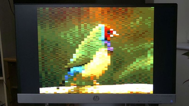
To be fair, [George Foot] does qualify his claim to the simplest usable VGA adapter, and he does note that it descends from [Ben Eater]’s “world’s worst video card”, which he uses for his 6502 breadboard computer. But where [Ben]’s VGA adapter uses about 20 TTL chips and an EEPROM, [George] has managed to decrease the BOM to just four TTL chips along with the memory and a crystal oscillator. This required a fair number of compromises, of course; the color depth is fairly low, as is the resolution. Each pixel appears as a thin horizontal bar rather than a small square, leading the images to be smeared out across the screen. They’re still surprisingly viewable, though, which probably says more about the quality of the pattern-recognition wetware between our ears than anything about the quality of the adapter. [George] gives a tour of the circuit in the brief video below.
It looks like [George] has posted a few improvements to the project since we first spotted it, so we’re looking forward to seeing how much the parts count went up. We’re also keen to see if anyone can outdo the simplicity of this effort — be sure to let us know if you give it a shot.


Not really a video card more of a testcard generator.
Fun non the less
Well use dual port SRAM, or get it to run off cycle with SRAM and it is a video card
The video generation does not care whether or not the VRAM is writable. Your comment draws a distinction without a difference.
Of course you can beat it: just replace the counters with a CPLD. And if you say that’s cheating because it’s programmable logic, what do you think the EEPROM’s being used as?
Video? TL;DW
if there are only four TTL chips, couldn’t you just say what they are?
Three counters and an octal DFF.
one 4-bit counter (pretty much any should work, such as 74HC93) as a prescaler from the crystal oscillator, plus two 8-bit counters, (possibly 74HC393), and one octal D Flip-flop (possibly 74HC373) to be precise.
Neato. This reminds me of something a friend of mine did as a poc a while back. Still always cool to see an image come up after its all done :)
Dan Lancaster would be proud!
Don
I just watched Bens video card a few days ago, and my first thought was also to put the sync signals in the ROM chip.
I was also surprised that the circuit worked at all with so few power connections between the boards and hardly any decoupling capacitors, and this article confirms it was indeed very marginal.
Ben also mostly shrugged his shoulders about the distortion lines at color changes, and [George Foot] addressed this nicely with the output buffer. This was probably out of pure necessity to clean up the sync signals which Ben did not have to do because they were generated by hardware counters and nand gates in his design.
I also like the extension with a RAM chip instead of EEprom so the video card can be updated while in use.
Next step into making it useful is some kind of bank switching, so updating a picture can be done while displaying another picture. Maybe some clever use can be made of the output buffer, to write to the Video RAM while the VGA data is buffered.
There is also a thing called Sync-on-Green. For Ben’s design it was not very important, as the sync signals were generated separately, but in this design the separate sync signals are a strain on the only 8-bit wide databus.
Sync-on-Green is (I think) a bit of a weird duck. I think it may not be an official part of the VGA standard, yet have a suspicion that (nearly?) all VGA monitors support it.
What would be the “simplest” is a moot question. I’ve seen video signals generated from just a few resistors on a microcontroller output. I quite liked Jerri Ellsworths commodore 64 on a single chip, and it may still be possible to buy VGA chips that do this. The answer would reatly depend on today’s definition of “simple”.
Using a small 320*240 TFT LCD with built-in driver chip is much more practical, but probably also skips the intention of projects like this.
When I designed my own VGA circuit I found that a latch on the output was critical to get rid of the weird colour lines.
The ram takes a little while to start outputting valid data for the next memory access so you end up seeing the indeterminate output displayed as those weird colour artifacts – Adding a latch clocked by the pixel clock makes sure the output is updated only when the signals have settled.
To get a good picture you need to consider the propogation delay of all components and make adjustments so the outputs all line up.
This is pretty impressive. Lots of action out of some very simple parts. It meets my definition of “running light without overbyte”.
Here’s my take on a “simplest” video system. http://www.sunrise-ev.com/vip2k.htm The VIP2K was designed using parts you could get in 1980. The NTSC video portion is just 3 chips; a 4040 counter, 2716 EPROM, and 74HC166 shift register. The whole computer fits in an Altoids tin. :-)
Good thing that he credits this to [BEN EATER]
https://www.youtube.com/watch?v=l7rce6IQDWs
I like it!
I have done a number of these but mostly with CPLD.
This is a great project type as an introduction to CPLD and a HDL – Veralog / VHDL.
They’re a good addition to a home built retro computer.
Being “retro” your probably going to use 5v chips.
You can cut the part count by using CMOS counters like 4040 – 4060.
Some things I have found on the way – though I used CPLD, most of this applies to the discreet chip design.
As mentioned you have the 5v hurdle. You can still get 5v tolerant CPLD for one off projects. These come complete with development boards in some cases.
For reference, the project in this article is equivalent to about 64 Macro cells but you could do the same in CPLD in about 30 Macro cells.
Xilinx XC9536XL XC9572XL XC95144XL are 3v3 chips with LVTTL outputs and 5 volt tolerant inputs and are 36 72 and 144 Macro cells respectively so they will work fine with 5v chips.
Altera EPM240 EPM570 are 3v3 chips with LVTTL outputs and 5v tolerant inputs. The data sheet specifies series resistors on inputs used for 5v signals but I never have used the series resistors and I’ve never had problems. These are about 190 and 440 Macro cells respectively.
If your new to HDL then the Altera design environment is easier than the Xilinx.
You can power these at 3v6 to improve noise immunity especially if your using a breadboard.
Alternatively you can use a modem 3v3 only CPLD aqnd lots of level translators but this is going to look very busy on breadboards.
Now to the actual logic stuff that almost equally applies to discrete and CPLD designs.
Lets say you want a color depth of 4 bits per pixel (bpp) or 16 colors. You may think to read from SRAM into an 8 bit buffer and then multiplex down 8 to 4 bits. That’s a waist of an 8 bit buffer (latch) and will introduce complex timing constraints because there is a delay on the read (of SRAM) with the 8 bit read that is different timing for the reading of the second four bits from the buffer. Just read the SRAM twice as often. Once for the lower four bits and once for the upper four bits. Alternatively, for 2 bpp read the SRAM 4 times as often.
Now that you know your SRAM read rate you can cut that time in half and allocate half of it to the VGA and half to the CPU so that you can use cheaper fast SRAM instead of duel port SRAM. Dual port introduces more problems than it solves. Cheap SRAM is down to 10nS now so it’s no challenge to an older 8 bit CPU.
Now to the CPU access side. Don’t get lost in complex timings. If the CPU is writing at a quarter of the rate of VGA reading then it’s perfectly fine to write data to the SRAM 3, 4 or 5 times as long as the same data is valid each time. The same applies to reading.
You can simplify things by deriving the CPU clock from a division or multiple of the pixel clock and that’s easy to do with 6502 like CPU’s but it becomes a mess to consider with variable clock cycle instructions (modes like refresh) on the Z80.
Read back from SRAM to a tristate 8 bit buffer and let the CPU control the buffer. Write through to SRAM transparently
So the over all picture is this – For every VGA read of the SRAM you also have alternatively a read or write opportunity for the much slower CPU. the CPU read is less complex. You can do a CPU read every cycle even if the CPU doesn’t want it because it just goes to an 8 bit buffer that the CPU has tristate control of so that it can read it when it wants. On the write sided you can only do a write when the CPU data bus is valid. If it’s not a valid write then do a read instead. Some simple logic can answer this question for your favorite CPU. Don’t worry if that causes multiple writes to SRAM or an odd number. As long as the CPU buses represent a valid write state then it doesn’t matter.
Timing schemes:- Modern VGA monitors don’t care about pixel clock frequency. The only care about HSYNC and VSYNC timing and polarity. You can use 800×600 V/HSYNC timings and output 512 horizontal pixels and they will be fine and cover the full line as long as they take the same overall period.
The number of vertical lines is a different storey. They have to conform to the standard related to the V/HSYNC signals.
I used CPLD development boards which often had an onboard 50MHz clock so I most often chose 800×600 72Hz (50MHz pixel clock) standard but my pixel clock would be 25MHz and I would repear each line twice so the end result is 400×300 72Hz – 25MHz pixel clock. Even 400×300 can be a bit much for a slower 8 bit CPU. You may want to try 200×150 72Hz – 12.5MHz pixel clock.
So while you have to use a division of the standard lines, you have more freedom with the horizontal resolution, you may want to try 300×300 72Hz or some other resolution that better matches your memory size block.
Another CPLD option is the Microchip ATF15XX series which are 5V and pin/code compatible with the Altera EPM7000 series. Just run the .POF through pof2jed and you get a Jed file for the ATF
I’m all for CPLDs, and sometimes even FPGAs, but either of these requires infrastructure, in the form of hardware to program the patterns into these devices, and software to generate the patterns in the first place. And sure, the same applies to Arduino – you need both a programming device, even if that’s just a USB-serial chip, and the development software, even if that’s the free and simple Arduino application. But nothing says “simple” better than wiring off-the-shelf devices together. Which this would be, if it used SRAM and had something in the way of address and data multiplexerx to add writing from another device. And those multiplexers don’t take that much more. So yeah, you’re going to be up to around a dozen chips before you have something that can be considered a complete graphics adapter, but it would be something that can be understood without needing to see the “source code”.
Even with limiting the design to “bread and butter” 74-series chips, the real limiting factor is the size of the EPROM (or SRAM as JockM suggests). While the counters can provide 16 bits of addressing, even if we assume that half the pixels are black for overscan, the 480×40 picture we see needs only 38,400 distinct locations, which in reality is really closer to 32,768, which coincidentally the capacity of a 32 kByte device. Which was probably the largest that George had on hand. Just like 25.whatever MHz was a convenient clock chip. But while 256 kbits (32 kBytes) was once a limit for cheap and available SRAM or EPROM chips, pretty much the only thing that limits this today is package size. 32 kByte seems to be as big as you can get in DIP. But if you can deal with using a breakout board, or other method of connecting surface-mount devices to breadboards, 64 and 128 MByte chips are available and cheap. Using a 128 MByte chip and clocking the counters from the 3.whatever MHz output of the prescaler would get you double the horizontal resolution, for 80×480, and by using one bit of the prescaler plus the 16 bits of the two 8 bit counters, the same SRAM would get you twice that again, for 160×480, without changing the chip count.
Other problems begin to occur when you’re counting to large numbers, such as the ripple count delay. This can be resolved by using synchronous counters rather than ripple counters, which can go much faster without taking so long for the result to settle. The penalty is that I don’t see any 8-bit synchronous counters in the 74-series pantheon. So taking this route would add two chips (replacing the two 74×393 counters with four 74×163), but it would reduce the amount of glitching caused by counter ripple. I haven’t done the math, adding up the maximum ripple delay, so I don’t know if this would be necessary for a 160×480 display.
That isnt “VGA” is more like a palette shifted CGA or EGA.
Amiga had that high multi-color VGA type of coloring before IBM clones cards did.
What exactly is the point of this… making tech out of deprec hardware?
Reinventing the wheels have zero purpose.
Why didn’t we finish adding on a USB FTDI chip to the Pano logics?
Why is anyone seeing we are being pushed back into the dark ages of technical literacy?
Intel swallowed Altera
NVidia swallowed ARM Holdings
AMD just swallowed Xilinx…
What is the point of these “just 4 chips”? Can it read and present a .pdf that has been blacklisted? Or is this someone looking for an ego stroking like so many other projects..
What is the point. Well, you have a very high standard for hobbyists. In the arena of technology, often amateurs and hobbyists don’t have access to the latest technology, because chips aren’t available in small quantities, or in many cases not at all. So while VGA is indeed a deprecated standard (for good reason in the case of flat panel displays, where the use of analog signals in the interface is obsolete since both the source and destination are digital), and as you say, this isn’t even VGA, it’s actually a step forward. A great many projects, even in 2020, rely on even older and poorer technology, composite color video, which is not just obsolete, but was just barely acceptable when it was new, and this project demonstrates how simply a video interface can be built that jumps the quality up by orders of magnitude, and allows plugging in to monitors that are being manufactured TODAY.
The point is that even though this is a truly lame implementation (heck, you can’t even change the picture without reflashing the ROM!), it demonstrates some useful techniques for simplifying hardware:
1) Generation of sync signals by embedding them in the data, allowing this to be taken care of in software with very little hardware.
2) Reducing high-soeed requirements by updating data at a fraction of the full clock speed while maintaining timing requirements.
3) Relaxing some requirements, such as the common desire for square pixels.
Yeah, maybe a stretch, but the first point was kind of a big deal. Sure, Sinclair managed this thirty-plus years ago, but only by using most of the resources of a microprocessor.
Are all of these things old hat to you? Then good for you. But you probably don’t advocate eliminating primary education, on the basis that you already know how to read, write, and do arithmetic.
And now you’re going on about how big companies are absorbing smaller companies? Let’s look at that. Xilinx and Altera, companies that require proprietary tools to use their chips. Yeah, what could go wrong there? Most hobbyists aren’t up to speed on synthesis and simulation of complex digital systems, and even when they are, what are you going to do about it? The tools for doing the logic synthesis are themselves dependent on knowledge of proprietary details about the architecture of the chips themselves. And anyway, again, what do you suggest doing about it?