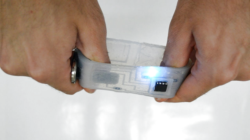
Flexible circuits built on polyimide film are now commonplace, you can prototype with them at multiple factories, at a cost that is almost acceptable to your average hacker. Polyimide film is pretty tough for something so thin, but eventually it will tear, and with larger components, bend radii are quite restricted. But what about stretchable circuits, as in circuits you can flex, twist and stretch? Let us introduce silicone devices. A research group from Hasselt University, Belgium, have been prototyping making truly flexible, silicone-based circuit substrates, managing to integrate a wide range of SMT component types with a dual layer interconnect, with vias and external contacts.
It should be possible to reproduce the process using nothing more special than your average Makerspace CO2 laser cutter, and a couple of special tools that can be easily made — a guide for that is promised — it is purely a matter of gathering a few special materials, and using off-cuts you have lying around for the rest. The interconnect uses Galinstan, which is a low melting point alloy of gallium, indium, and tin. Unfortunately, this material is fairly expensive and cannot be shipped by air due to the gallium content, without specialised handling, at considerable expense. But that aside, other than some acrylic sheets, some vinyl, copper foil and a few sprays, nothing is beyond reach.
The construction process is reverse to what we normally see, with the components and copper contact plates placed first, on to a primed vinyl sheet. This sheet is laser marked with the component outlines to enable them to be corrected placed. Yes, that’s right, they’re using a laser cutter to mark vinyl, a chlorine-containing plastic. Hold on to that thought for a bit.
Insulating layers and substrate layers are constructed by blade-coating with a layer of clear silicone. Interconnect layers are formed by sticking a fresh vinyl sheet onto the exposed contacts and laser cutting just though it to expose the pads and the interconnect traces. Next the fancy Galinstan is applied by brush and the vinyl stencil removed. Rinse and repeat for the next layer of insulating silicone, more circuit traces, then use the laser cutter to precisely etch through the via regions to allow more metalisation to be added. Finally a coating of silicone is applied over the whole assembly, the laser is again used to etch the silicone away from the contact pads, and with a little solder tinning of these, you’re done. Simple, if only our Makerspaces didn’t have rules against laser cutting vinyl.
This was clearly a very brief overview, here is a very detailed instructables guide ready for you, as well as a formal research paper, detailing why this came about and why you might want to try this yourself.
If you’re into custom wearables, you might remember this earlier piece about silicone circuits, and this one weird organic-looking thing from the same time-frame.
Thanks [Daniel] for the tip!


How about chopped carbon fiber or graphite powder in soft silicone, if we can trade some conductivity for not needing an MSDS: https://www.instructables.com/Conductive-Rubber-Make-Touch-Sensitive-Robot-Skin/
Galinstan also has the benefit of being a heat-conductor, as well as being a good (electrical) conductor. -19 C is a really good temperature for flex circuits, and it self-heals once reheated
The hundreds-ohm-scale resistance is pretty brutal on that, though it seems that there wasn’t any reason for them to try and optimize conductivity in that example (or perhaps even motivation for them not to). It could work really well. The only issue I can see is that then both the substrate and the conductor would be rubbery and thick. You’d need to figure out a good way to define the boundaries as you poured and scraped the stackup. I imagine you’d want to partially cure thin conductor traces, then scrape the substrate layer over it for each layer of the stackup so you wouldn’t smear the trace.
This would make for manufacturing without masking, though consistently extruding thin beads of silicone compound would be the achilles’ heel of the process, and would seriously detract from the scalability of the process, something the researchers for this process emphasized, and is extremely important to commercialization. I’ve done some work with automating extrusion of sealants and adhesives, and even with extremely loose tolerances for the result, qualifying the systems is always a nightmare. The thickness and consistency of the beads would also be the limiting factor for stackup optimization.
What would be really cool would be a quasi-3-layer stackup. You could have the outer layers with the bead traces facing outwards, with a very thin silicone mask, and then the middle layer being a very thin conductive layer for return paths. Of course, this would only work well if conductivity could be massively improved from the project you linked, as even a perfectly uninterrupted ground plane is useless for return paths if its impedance is sky-high anyways.
What about resistance? I remember HaD had a video on the development of a stretchable conductor and the big problem with them is that when you stretch it then it was prone to change in resistance. However, they had found some chemical that didn’t have that problem. I wonder if that chemical was Galinstan.
I was thinking you could have copper wired bent into a zig-zag shape and embed them instead, cheap and effective.
What if you do loops? Resistant to being stretched in all dimensions. I thought of zigs too, but what happens if you stretch them sideways?
“…cannot be shipped by air due to the gallium content…”
Wrong. I teach IATA DG Regulations for an airline.
You can ship up to 20kg of gallium in a single package by air as long as it’s properly packed and declared. It’s a Class 8 Corrosive.
… without specialised handling, at considerable expense.
Says the rest of the sentence. Yes, it can be shipped, but at what cost? and that cost is passed on to the end customer. I would be very interested in an actual figure to ship a small quantity according the appropriate regs.
That is very neat, though I would wonder how long it will take the liquid metal traces to work their way through and short out the SMD components as its stretched etc, it might be fine for a very very long time or significant stretch distance without any harm at all, that sort of casting silicone sticks to itself even fresh batch to long cured stuff really damn well and is pretty tough, but that is still a rigid object in one layer shifting relative to the conductive trace layers with only a small discontinuity in the traces – as even large for SMD are not really all that big – maybe using discreet components with their longer bodies?
Still as flexible and durable let alone stretching, flexing and durable electronics are relatively challenging and rare this rather simple (if you have the tools at least) method looks like it has a great deal of potential and being sealed in silicon will have many uses the more fabric based sewing/weaving with wire or screen printing conductive/semi-conductive trace type methods won’t be a good fit for.
Have you considered using PolyLMN? https://hackaday.com/2020/11/19/circuit-boards-you-can-stretch-liquid-metal-nanomaterials-make-a-strange-flex/ They now sell sample quantities of the materials if you are interested. Not really difficult to pattern and bake.
My first idea on how to do something similar on the cheap would be to use wearable techniques, sew each trace with conductive threads in zig-zag elastic stitches on a silicone “elastic” (lastin) layer, solder the smd parts, and sandwich the layers between silicone pours. Or something like that.
Aaand now I want to try… Damn you Hackaday, always extending my never-ending list of project ideas! 😆
How did you get the gallinistan to stick to the pdms? Mine has very low wettability!!