There was a time when the very idea of building a complex circuit with the intention of destroying it would have been anathema to any electrical engineer. The work put into designing a circuit, procuring the components, and assembling it, generally with point-to-point wiring and an extravagant amount of manual labor, only to blow it up? Heresy!
But, such are the demands of national defense, and as weapons morphed into “weapon systems” after World War II, the need arose for electronics that were not only cheap enough to blow up but also tough enough to survive the often rough ride before the final bang. The short film below, simply titled “Potted and Printed Circuits“, details the state of the art in miniaturization and modularization of electronics, circa 1952. It was produced by the Telecommunications Research Establishment (TRE), the main electronics R&D entity in the UK during the war which was responsible for inventions such as radar, radio navigation, and jamming technology.
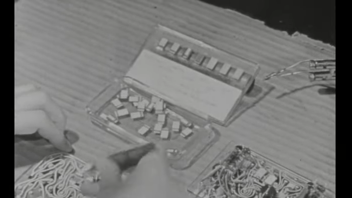
The first bit of the film below focuses on circuit potting. The circuits shown are built “cordwood style”, meaning that axial-lead resistors, capacitors, and inductors are mounted between two flat plates and wired together with short jumpers. It was a tedious and time-consuming construction method, but had the virtue of mechanical strength and low material cost. The potting process that followed was just as tedious, with mica-impregnated polyester resin being added to the circuit after mounting it in a mold. The resulting brick was un-molded and active components, which at the time meant vacuum tubes, would be mounted externally and wired up separately.
Where things get really interesting is in the printed circuit production process, which at the time took the “printed” part very much literally. Rather than etching copper from a pre-clad board to create traces, a die of the traces was built up from steel tooling, referred to as “type” in a nod to the printing industry, and used to press silver powder into traces onto a phenolic substrate. On the other side of the board, resistors were created by etching an even layer of graphite powder using shot blasting. And if all that doesn’t pique your interest, wait until you see the glass boards — not fiberglass, but actual glass.
For a construction method intended to make circuits cheap enough to blow up, everything shown here is fantastically labor-intensive. Then again, it was just after the war, and labor was probably pretty cheap, and when have governments ever been shy about throwing money at arms makers? Plus, it was more likely that robustness and reliability were the true imperatives driving these methods.


At the other end of things, look at IBM’s Thermal Condition Module some time — sintered many-layer ceramic boards PCBs with shrinkage precisely enough controlled that bipolar chips could be directly surface mounted to them, then wrapped in a fancy helium-filled/spring-loaded case that was able to extract heat from those bipolars fast enough to prevent their cooking themselves when bolted to chilled-water heatsinks. General reaction in the industry when this was announced was shock that it had been made to work.
TCM teardown: https://www.youtube.com/watch?v=xQ3oJlt4GrI
At 19:25 it shows the earliest example of a plug-in cartridge that I’ve ever seen.
Anybody noticed at minute 5:45 how they put the potted component in “boiling” water, but the you can see its cold water with dry ice in it?
That trick with pressing / heating the silver powder to fuse it into traces is just wild!
Wonder if you could do a laser-sintering equivalent process today? 3DP meets PCB.
At 18:17 they show off carbon resistors that they’ve printed directly onto the PCB substrate that look a lot like modern SMDs today. It’s wild that they developed a process that could easily mass produce components but instead of figuring out how to make them discrete they instead decided print in place was the future. At around 21:00 they propose printing the resistors and low value capacitors directly onto the PCB substrate shifting their manufacture from the OCM to the ODM.
Clearly this never caught on because having a passive permanently attached fail on a device was much more expensive to repair than discrete components.
It was another 30 years before SMD was adopted.
Only ten years after this movie.
https://en.wikipedia.org/wiki/Surface-mount_technology
“Surface-mount technology was developed in the 1960s.”
Keep in mind that the video in this Hackaday article is about research. It is not about finished production methods. It’s about learning the things that will need to be done to make the machines and the processes that will be used in production.
At 14:00 “since errors cannot occur in printed wiring inspection is unnecessary at this stage.” It’s kind of cute that they thought this way in 1952.
Realistically I think they meant that there was nothing that could be done to rework errors at this stage so no point in inspecting when a final function test would weed out any bad units.
These days we would inspect after every step and use the resulting manufacturing data to drive down defects produced in that step but in 1952 such data driven quality management practices had not yet diffused from academia to industry.
I suspect any competent production manager at the time would be aware of some of these ideas and might practice some subset of them. After all Walter Shewhart (https://en.wikipedia.org/wiki/Walter_A._Shewhart) first advocated early inspection and control charts at Western Bell in 1924 and W. Edwards Demming (https://en.wikipedia.org/wiki/W._Edwards_Deming) met him at Bell Labs in 1927. Demming went on to develop and proselytize statistical quality methods during and after WW II but the first significant non-military industrial interest seems to be among the Japanese industrialists Demming was brought over to help rebuild Japans industrial base under McArthur’s tenure running Japan.
US manufacturers finally got the quality memo in the 1970’s when inexpensive, reliable Japanese cars and electronics started seriously threatening the market share of major US manufacturers.
Apparently British industry, at TRE anyway, in 1952 had not adopted Shewhart’s 1924 ideas about control charts and inspections nor integrated Demming’s ideas about quality management.