Today, we revisit another board from [Exentio] – a HDMI/DVI to LVDS transmitter for the Sony Vaio P display. This board is cool to review – it has a high-speed serial interface, a parallel interface, a healthy amount of power distribution that can be tricky to route, and many connectors to look over.
I’ve decided to show this review to you all because it demonstrates a PCB improvement concept we haven’t yet touched upon, that you should absolutely know about when doing board layout. Plus, I get a chance to talk about connector choice considerations!
The board is lovely. It integrates the DPI-LVDS circuit we’ve previously reviewed, but also a HDMI to parallel RGB chip from Texas Instruments, TFP401, a chip appreciated enough that even Adafruit has adapters with it. The fun thing about this chip is that it doesn’t even handle EDID like the usual HDMI to RGB/LVDS chips you get on cheap Aliexpress boards. So, there’s no firmware to take care of – it just receives a HDMI/DVI signal, converts it into parallel RGB, then converts that to LVDS, and off to the display it goes. The downside is that you have to provide your own EDID with an EEPROM, but that isn’t that tricky.
Again, this is a two-layer board, and, again, I like this – fitting tracks to the smallest possible space is a respectable and enjoyable challenge. This board has absolutely done well by this challenge. I do see how this board could be routed in an even better way, however, and it could be way way cleaner as a result. For a start, rotating the chip would improve the odds a whole lot.
The Chip Gets Rotated
When doing silicon layout, engineers generally try and make the resulting chip pinout as sensible as possible. There can be exceptions, of course. This rule means that there’s usually a single easy way to lay out a chip, and a few hard ways. You have to look at the pinout, try to notice the pin groups, and see how they align with your peripherals. Ignore this at your own peril.
The TFP401 chip has HDMI on one side and parallel RGB pins on the other. This board, however, currently has the chip rotated in a way that disadvantages the layout. This is an easy mistake to do initially – thankfully, even when the design is already finished, rotating the chip and rerouting it can pay off!
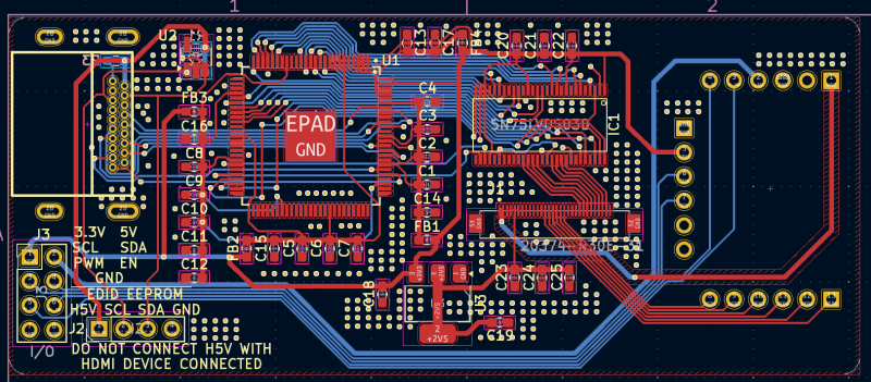
If you reroute this kind of board, not only you are more likely to get a functioning board, considering the high-speed signals, you’re also training yourself to distinguish good and subpar chip rotations as you’d be rerouting. In other words, it’s the kind of refactoring that makes you say “wow, that was way easier than the first time around”.
Lift, Clean Up, Rotate, Behold
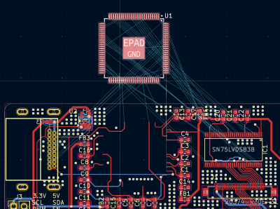 To do the reroute, just, take the chip, “lift it up” with
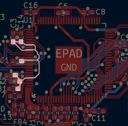
 M and move it off the board. See the grey thin wires? They’re called ratsnest wires, and using them is the best way you can notice rotation issues. Seriously, the ratsnest wires are underrated in noticing such issues before they bite you. Let’s clean the chip’s surroundings up. First, see those capacitor groups? Move them away too, all the power pins are changing their locations anyway, we’ll reposition them later.
Box select the signal traces that previously went to the chip, and press `Shift+Del` to completely delete them from beginning to end – on this board, this is the quickest way to get to a quickly routable space. Every trace that went to the chip is now gone, and every unrelated trace stays. Make sure there’s a healthy amount of space between the chip and the HDMI port, but also between it and the DPI-LVDS converter – more or less the same center position is fine here.
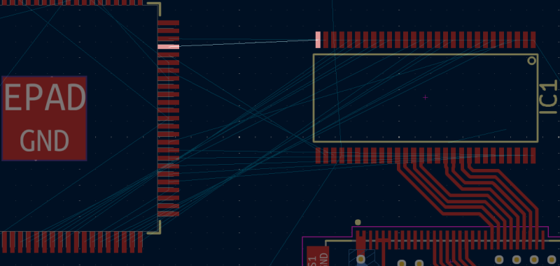
 Look at the picture above. Using the ratsnest wires, you can instantly notice which trace groups you will need to flip and which you won’t. In this case, as you might notice, you will need to flip like, three out of four? No matter, because all of them will be easy, even the HDMI pairs.
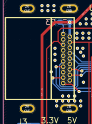
Speaking about HDMI, before routing, I will replace the THT signal pin HDMI connector with an SMT signal pin one. They’re way, way nicer to layout – the through-hole staggered pins mean that you have to run two of the diffpairs around the connector shell. Plus, they’re cheaper and easier to source too. [Exentio] picked this connector for expected sturdiness and solderability, and that is a valid choice, I’m just prioritizing ease of layout and easier sourcing.
Reroute Time
With HDMI, not only is the order flipped, but the pair polarity is also flipped. Still, there are multiple things you could do here. You could flip the connector onto the opposite side of the board, or use a HDMI connector that’s flipped (harder to source but not impossible), or try to re-route the diffpairs as they are now. I’ll do the last one, since it’s the most fun one.
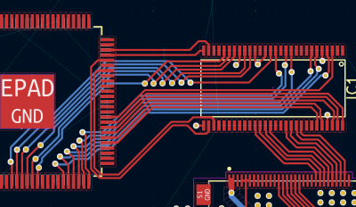
 Here’s my take. This is draft routing, without any calculated trace impedance, because this is a 2-layer board and we’re winging it. Still, I’m trying to give this routing some love – not that HDMI would ever love me back, I just think that this board working on the first try is a good goal to strive for, and HDMI can be sensitive. Pair length is also kind of matched between the pairs – they’re all 23 mm +- 2 mm, good enough. By the way, KiCad 8 has added a new feature where you can check track length by simply pressing 7 (8 for diffpairs) and then hovering over tracks – inter-pair length matching is now the easiest it’s ever felt!
Now, what’s left is three bundles of parallel wires (R/G/B) and four individual tracks (EN/CLKIN/HSYNC/VSYNC) going to the DPI-LVDS chip. Since all four individual tracks are on the DPI-LVDS chip corners, I’ve decided that the parallel RGB pairs will go in the middle and the tracks will go around them. The biggest problem is flipping the bundles – you can do that under the HDMI chip or under the LVDS chip, I did it under the HDMI chip because it felt like there was just enough space there.
Here you can see how the three bundles progressed. They’re nice and tight, with some ground fills between the separate bundles and accompanying the wires. I’ve had to move the first bundle once to make room for flipping the last one, but other than that, things fit surprisingly nicely. The bundles don’t intersect each other’s paths, and that helps. If they did, I would probably consider rotating the DPI-LVDS chip together with the LVDS connector.
 There are some other small tweaks too. I’ve moved the EDID EEPROM towards the HDMI I2C header at the bottom, only leaving the HPD pullup near the HDMI connector. The near-connector position is also a valid choice, I just wanted to do via-less routing of I2C as much as possible, and moving the EEPROM helped. Oh, and I’ve moved the LVDS connector to the right a bit – that let me route LVDS better, which, in turn, let me actually connect the DPI-LVDS chip’s 3.3 V pins.
Power Pin Routing
This is the thing you might get stuck on, at some point. The chip has whole four different groups of power pins – one direct 3.3 V input, and three separate 3.3 V inputs that you’re supposed to feed through Pi filters, for a cleaner power supply for all your analog needs. Use the “ (~)` key to highlight all four power nets of the chip – here’s how it will look.
I’d describe these as annoying, but they’re still routable. First, break apart the nice cap groups for the four rails – they’re nice visually, but they’re not great for power delivery. Remember – one capacitor per IC power pin is the platonic ideal, and each of these capacitors has to actually be placed close to a power pin, with a short path to ground too.
I started with the 3.3V feed, and then placed a couple of ferrites to nearby power rails. Then, I went through each of the power rails, starting with the simplest, pulling power tracks where it seemed viable. In the end, I could place all the ferrites near the actual 3.3V supply point. A 3.3V power plane could be fun on this board, and would probably be very much called for if we wanted to do FCC testing for this board, but for now, it’s not required.
Long story short, here’s the “rest of the owl” pictures. Remember – for power tracks, wherever you can make them thicker, make them thicker. They will drop all that less voltage, and they will look like dedicated power tracks, too. Also, don’t forget about GND! Highlight the GND net, then make sure that each GND point has a via directly near it, going to the bottom layer ground plane, with ground now even more abundant than before.

After this layout was done, there were only cosmetic fixes left. Things like trace keepout that I’m still maintaining, feeding 3.3 V everywhere it was called for. I suppose I would add a 5 V to 3.3 V linear regulator footprint onto this board, just because it would make bringup much easier, but it’s such a small change that it could even be bodged onto this PCB later with little hassle. This board is, all things considered, wonderfully hackable already.

Closing Statement
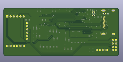
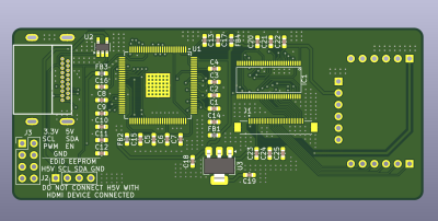
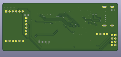
Here’s the end result of the board re-layout. It’s even cleaner than before, with improvements to both high-speed tracks and power distribution, and I hope it’s been a fun example about rotating your chips properly, something you could reasonably overlook on a board of yours.
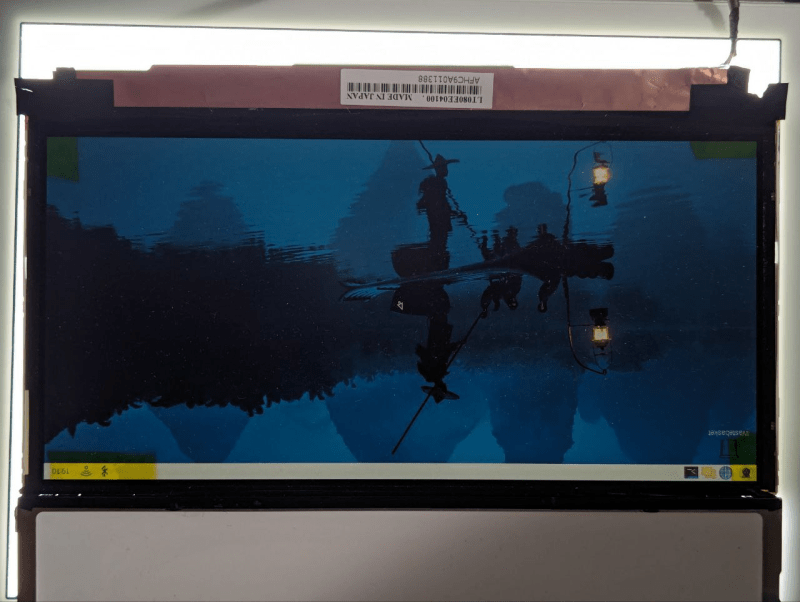
As an outro to this review, here’s some good news. That DPI-LVDS board we’ve reviewed last time? It works! Which means that the DPI and LVDS parts of this HDMI-LVDS board should also work. Nothing is fundamentally broken to the best of our perception, [Exentio] has designed a working RPi config, and, as such, one of the more challenging parts of the Sony Vaio rebuild design is now complete – we only need to tinker with the backlight now.
As usual, if you would like a design review for your board, submit a tip to us with [design review] in the title, linking to your board files. KiCad design files strongly preferred, both repository-stored files (GitHub/GitLab/etc) and shady Google Drive/Dropbox/etc .zip links are accepted.









i still miss the shortcut to change track thickness on the fly after routing. now you have to open a separate modal dialog to change them. or is there a shortcut for that?
Changing track width after the fact is a nuicance, even if there is a quick function to do it. It messes up clearances too. It is often the result of beginner mistakes. If you have a bit more experience, you usually learn to plan ahead, set up the design rules and use the correct track widths in the first place.
Also note that a 0.2mm track can already handle several hundred mA DC, and higher peak currents. Usually the width of nearly all tracks is determined by the resolution of what your PCB manufacturer can make (cheaply). 4-layer PCB’s regularly have a higher resolution then 2-layer PCB’s.
But if you want a shorcut:
1. Select a track segment.
2. Press u to expand the selection.
3. press e to edit the selection.
4. Fill in a new track width.
Another option is to use: PCB Editor / View / Show Properties Manager. This is a semi permanent dockable window that gives you quick access to the properties of the current selection.
I already do those things, it’s more when you route a power track to a chip with narrow power pins that you change the width for the last part to get to the pin. and sometimes you cannot squeeze enough tracks though a narrow space, so locally you make the tracks narrower. and of course you keep pressing B to update your zone fill.
but yeah. no right mouse click on a track to change its width.
wait, if you’re routing a power tracks to a pin, wouldn’t you be doing it on the fly with W/Shift+W?
High light the whole track by clicking one segment. Hit ‘u’ a few times to progressively select the entire track. Hit ‘w’ to cycle through your pre defined trace widths.
At least I think that works
Sorry, what software is this?
KiCAD
You could even use an inline EDID with HDMI passthrough if you were feeling suitably hacky. I use them to prevent windows cycling the outputs off and on when the displays on the splitters power up.
Many thanks for your series of article about video interfaces, I find them extremely interesting.
About the diff pair routing you showed, I would route them to try to prevent crosstalk by avoiding crossing pairs on the top and bottom layer. There is a way if you start with a 90° turn down, then go to the bottom layer and make them do a “U turn” after being below the QFP chip, and going to the top layer again. Writing this, I realize it’s hard to explain it with text… But this way they never have to cross each other, and you can keep them relatively far away as well. This also allows to couple them to a gnd plane.
Next step would be to try to have some impedance matching. It’s possible to try on a 2 layer board. Having thick traces and thin PCBs (like 0.8mm PCB thickness), you could maybe land around a +/- 20% impedance error.
But really the solution here is to go for a 4 layer board. It’s cheap nowadays and makes everything so much easier. It allows to put a ground plane on an internal layer which has 2 advantages:
– you can isolate top and bottom traces easily (also useful for non differential pairs, I’d like to see the crosstalk between these long DPI traces on top and bottom layer going bellow the LVDS transmitter)
– these internal layer are really close to the external ones (something like .1 or .2mm), this allows to design thin impedance matched traces that are easily compatible with the .5mm pitch of the IC without impedance discontinuities
Nevertheless, your board works so I guess everything I wrote isn’t really relevant. I’m just a bit obsessed with routing.
This specific HDMI board isn’t yet known to work, and, I appreciate your comment – it’s exactly the kind of comment I like receiving ^_^
About the diff pair routing – I’d seriously appreciate a Paint picture or anything! I always like new routing tricks, this one is a bit hard to visualize from a text description, but the way you talk about it, I’m intrigued!
Agreed on impedance matching, +20%ish on 0.8mm+thick traces sounds realistic to me too, I’ve done that on some 0.8mm 2L M.2 card boards of mine. And, of course, fully agreed on 4 layers, cross-talk and all – the final Vaio-integrated PCBs will definitely be 4-layer, if not more. I do like doing 2-layer designs like this, not only are they easy to turn into 4L whenever needed, but the routing constraint is fun to do, too!
You’ve done it already with one of the diff-pairs – instead of trying to connect all the pairs outside-to-outside directly, make sure each pair has one end that starts from the other side of the pad (i.e. going under the IC) before doing a u-turn back towards the destination. Since the pairs are in reverse order as well as flipped, all the crossovers essentially cancel out.
I did a rough routing example, I can send a picture to you somewhere?
That upside shot of the LCD was really confusing me. Until I realized it was a top taskbar and a reflection of the boat in the water. XD. Ya got me X’D.
This is awesome awesome stuff. Maybe one of these days the iPad Mini 1 screen will be available. 7.9″ and 1024×768 is just begging to be lashed to a cheap mechanical 60% with a Pi or Vortex86 thin client (now that we have that sound blaster emulator) or NUC or Framework or SteamDeck motherboard (boy are we spoiled for choice.)
Length matching the tracks is really easy to do. I just drew a pin header to pogo pin testing fixture and length matched all the tracks to 40mm very easily and that was my 3rd time using Kicad. Just click with the tool, select the next point to define the length of the meander. Then from the properties you can trim the length of the route and it will adjust the meander to match that. And as seen somewhere else, no crosstalk if the meander is with more than 3 trackwidths distance away.
I’m not an electronics engineer, but I was told that sharp corners are bad for high speed signals. Is that also the case for the via’s? Like in the first picture after “reroute time”, there are vias where the trace takes a 180 degree turn. Is that a problem or not?
Nah, sharp corners are basically completely irrelevant, a measure that had an original physical justification (etchant would collect in the corners and cause overetching) that someone mistakenly came up with a signal-integrity explanation for and the old-wives-tale was started. Nowadays it’s generally just an aesthetic measure.
Vias *can* however have implications, usually because they pass through layers and locally violate impedance rules, and designers can inadvertently create spurs and things they normally wouldn’t do on a single layer. Often datasheets provide explicit routing examples for high-speed signals that are sensitive to this.
Ah, thanks! Always good to learn. And can’t argue with aesthetic, a well routed board is a work of art.
From a newbie perspective this article is really interesting but it looks like a total waste of time.
I can’t help to wonder why there’s no IA or automatic graph solver that can do all the hard work for us ?
Why can’t we just express our constraints and let the solver optimize for the size/shape of pcb, its number of layer, ease of soldering, whatever.
Or better just do nothing but choosing components with their constraints.
Or even better don’t even select the components but just say what you want to do
” receives a HDMI/DVI signal, converts it into parallel RGB, then converts that to LVDS, and off to the display it goes.”
How far are we from this goal ?
“How far are we from this goal?”
Very far.
There’s a lot of autorouters for PCB layout available. The general consensus is that you only use them if the time it takes to define the constraints is less than the time it would take you to route the PCB manually.
In practice, that means really, seriously complicated things like a PC motherboard PCBs are designed using autorouters, and nearly nothing else. It takes a lot of effort to gather all the constraints and express them so that the autorouter can do something reasonable with it. Because of the amount of work you have to do, it is only used on complex designs that you expect to have to modify (revise.)
>even better don’t even select the components but just say what you want to do: ”receives a HDMI/DVI signal, converts it into parallel RGB, then converts that to LVDS, and off to the display it goes.”
Even further from that.
How should your design tool know which ICs to use? Maybe a new IC that does it all in one step, but is only available in low numbers for prototyping and there’s no information about future availability or quantities? Maybe something based on an FPGA but which is too expensive for mass production? Maybe something made of 40XX series CMOS ICs because they are common and available and cheap – but it’ll take like 5 bazillion ICs and a truly monstrous PCB? How about a solution that uses ICs that were common and cheap last year but which have gone out of production so that only current stocks are available and running out?
“I want to take a HDMI/DVI signal and output it as LVDS”
batch size : 1
pcb size: low priority (indicative size : 2 inches * 1 inch)
ratio: square
max width : 10 inches
max length : 5 inches
price: top priority (indicative price for BOM: <20$)
# layer: don't care (4 layers ; current solution needs at least 2 layers)
Your input : HDMI/DVI
Your output : LVDS
Your logic : possible alternatives
1) use lot of ics (pro; cheap; con: complex routing)
2) use fpga (pro: efficient; con: pricy)
2.a) STMxxxxxxx
2.b) Xilinxxxxx
See complete list of FPGA capable of processing a video signal of 1920*1080@30
3) use all-in-on ic (pro: efficient; con:pricy)
3.a) TI400xxxxxxx
3.b) STxxxxxxxx
configure input :
rule : supported resolution : 1920*1080 @ 30hz and standard
connector : possible alternatives
1) hdmi connector (pro:: standard, usefull for outer world; con: pricy)
2) raw pins (pro:cheap)
configure output :
1) lvds connector (pro:: standard, usefull for outer world; con: pricy)
1.1) 30 pin connector
1.2) 40 pin connector
2) raw pins (pro:cheap)
configure input voltage :
1) 3.3 V
1.1) raw pins
1.2) add barrel on pcb
2) 5 V
1.1) usb A
1.1.1) add micro usb connector
1.1.2) add full size usb connector
1.2) usb C
3) PD
….
That’s a far cry from ”receives a HDMI/DVI signal, converts it into parallel RGB, then converts that to LVDS, and off to the display it goes.”
It still requires you to have some understanding of what is involved. As asked, the intent was to do away with understanding it at all and just palm it all off on some automated system.
Your solution shows again just how silly an idea it is to have a system that just does what you ask for. The list of parameters that you’ve made up are in no way obvious if you don’t know anything about electronics.
For me those are lego bricks vs Acrylonitrile Butadiene Styrene molecule.
This should be seen as an iterative process.
The IA shows you what are the options at every stage and you stop digging deeper (= going to the next stage) when you don’t understand anymore or when you didn’t care.
You : “I want a pcb that converts HDMI/DVI to LVDS”
AI : Here is your KICAD file.
I made the following assumptions :
INPUT : hdmi connector
OUTPUT : LVDS 40 pins
Max resolution : 1980 * 1020 @ 30 fps….
Here are the different stages that I identified
Power \
amplification -> conversion -> output
input /
> move “amplification” to top right of PCB
rebuilding KICAD, moving “amplification” block to top right. done.
> “Power.inputvoltage” = 3.3
rebuilding KICAD. Done.
> “amplification”
…
optimizedfor:”price”
maincomponent:”XYZ12″
…
> “conversion.stages”
hdmi to RGB -> RGB to LVDS
> “conversion.stages.hdmi to RGB”
…
optimizedfor:”price”
maincomponent:”XY”
…
> “conversion.stages.hdmi to RGB.maincomponent” ?
Alternatives for XY are : STM7, TI1…
> “conversion.stages.hdmi to RGB.maincomponent” = STM7
Rebuilding Kicad. Done.
Routing is simultaneously a creative design problem as well as a graph routing problem. The latter can have a mathematical solution (albeit one that runs smack bang into complexity issues) whereas the former doesn’t. The search space is huge, and we have design constraints we can’t even adequately put into words let alone describe to an algorithm.
AI may do a better job of this in future, but realistically the end results have always been superior if you learn to do it yourself. Autorouters have a place as a convenience tool if you have a mostly routed high-density board and are trying to thread a single signal through the forest, but even then a designer will only use the result as a starting point.