When we think of machine learning it’s usually in the context of robotics—giving an algorithm a large set of input data in order to train it for a certain task like navigation or understanding your handwriting. But it turns out you can also train a nasty virus to go to sleep and never wake up again. That’s exactly what the Immunity Project has been doing. They believe that they have a viable HIV vaccine and are trying to raise about $25 million to begin human testing.
The vaccine hacks the Human Immunodeficiency Virus itself, forcing it to mutate into a dormant form that will not attack its human carrier. It sounds so simple, but a lot of existing knowledge and procedures, as well as new technology, went into getting this far. Last week we spoke with [Reid Rubsamen, M.D.] about the process, which began by collecting blood samples from a wide range of “Controllers“. Controllers are people who carry HIV but manage to suppress the virus’s progression to AIDS. How do you find these people? That’s another story which Scientific American covered (PDF); the short answer is that thanks to the work of [Bruce D. Walker, M.D.] there was already a database of Controllers available.
The information accumulated by [Walker] then underwent a data crunching exercise. The data set was so enormous that a novel approach was adopted. For the laymen this is described as a spam filter: using computers to look at large sets of email to develop a complex process for sifting real messages out of the noise. The task at hand is to look at the genotype of a Controller and compare it with the epitope— a short chain of proteins—in the virus they carry. The power of machine learning managed to whittle down all the data to a list of the first six epitopes that have the desired dormant-mutation property. The vaccine consists of a cocktail of these epitopes. It does, however, require some clever delivery tactics to reach the parts of the world where it’s most needed. The vaccine must not require refrigeration nor any special skills to administer.
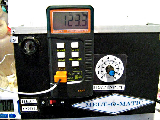
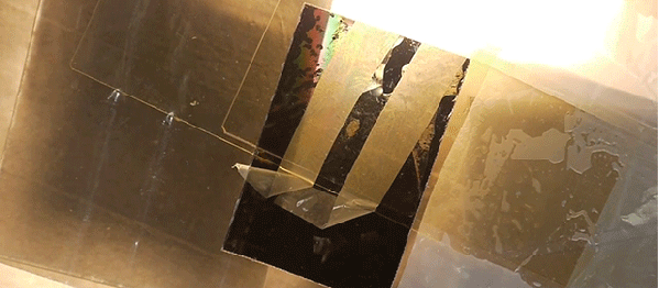
The vaccine’s production uses existing methods to synthesize the amino acid peptides, which are the epitopes themselves. The packaging, however, is a new concept. [Dr. Rubsamen’s] company, Flow Parma, Inc., is using microspheres to encapsulate the vaccine, which render it shelf-stable and allow it to be administered through a nasal spray. Learn more about the technology behind the production of microspheres from this white paper (PDF).
If the vaccine (which will be produced without profit) passes clinical trials, it could see mass distribution as early as 2017.
The $25M we mentioned earlier is a tall hill to climb, but think of the reward if the vaccine is successful. You can donate directly to help reach this goal. If you’re planning on giving gift cards this year, you can purchase them for many different retailers through Gyft, who is donating 100% of December proceeds to the project.