Having the information shown on the display of a digital multimeter also recorded off-screen can be incredibly useful, but unless the device exposes something like SCPI on a network interface, you will have to get creative. In the case of the budget ANENG AN870 digital multimeter (DMM), [Bits und Bolts] really wanted to show its display clearly as an overlay in OBS instead of just the camera view, but with said DMM not offering an easy way he had to resort to just copying the data sent to its multiplexed LCD.
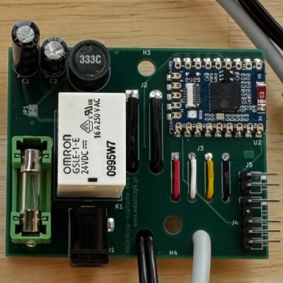
The GitHub project page contains the background information, as well as the instructions if you too have this DMM. It might of course also be useful as the jumping off point for your own DMM modification. In total the project requires three modules: an RP2040 Zero and HC-12 433 MHz transceiver on the DMM side, and another HC-12 plus ESP32-C3 module on the receiving side. A boost module is also added to generate 3.3 V out of the 2.4 V – 3 V provided by the meter’s two AA cells.
To be able to read the LCD signal lines, a custom PCB was created that is installed inside the DMM. With the LCD’s segments mapped, this meant being able to send a perfect copy of the display’s state to the ESP32-C3 and from there making it available via WiFi.
Continue reading “Wireless LCD Streaming For The ANENG AN870 Multimeter”


 Even with Amazon’s Echo Show devices running Linux in the form of the Android-derived FireOS, using them for non-Amazon approved purposes can be a chore at best. In the case of the Echo Show 8 even simple workarounds using ADB and the bootloader have been locked-down, requiring more drastic measures. Here [Vowed] over at the XDA forums shows off one such hack, involving