
As simple as the concept of adding two numbers appears at first glance, doing it in the 1970s in Intel’s 8087 FPU with its 69-bit adder was still a tall order. This is namely the core feature that many features like tangents, cosines and exponentiation rely on, so it had to be basically perfect. In a recent die-level analysis of the 8087 [Ken Shirrif] dives into the structure, layout and functioning of this ‘beating heart’ of this piece of semiconductor history.
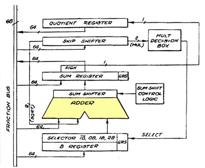
Although anyone can build a simple binary adder out of off-the-shelf parts including 74-series logic ICs, the problem is to make it fast so that the 69th bit doesn’t have to wait for e.g. a carry to trickle all the way through the preceding bits. The main way that this is solved is by breaking addition into 4-bit blocks, reducing the problem by a factor of four, along with an optimized Manchester carry-chain carry-lookahead implementation.
The main advantage of this variation of a carry-lookahead is that it reduces the number of required transistors, without sacrificing too much performance. Later on Intel would switch to the faster, but more transistor-intensive Kogge-Stone adder.
Implementing this entire adder with NMOS technology and wiring it all up to the rest of the die required a lot of ingenuity on the side of the Intel engineers, as previously noted this adder is effectively always used in any operation at some stage. This necessitates many surrounding registers and in turn circuitry to manage these, with part of the complexity handled in microcode and part in silicon.


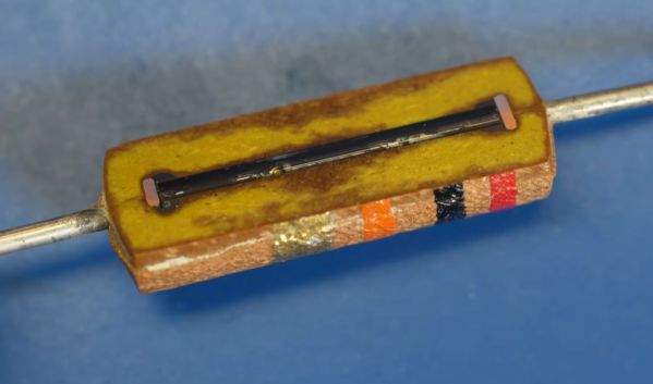
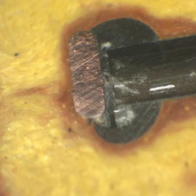
 The Honeywell X2S Smart Thermostat is a Wi-Fi-enabled thermostat that is meant to integrate with your typical ‘smart home’ setup, with mobile app control available as well. Of course, just using it as-is would be extremely boring, so fortunately we have [author0] to take it apart and


