Working under the pressure of being watched on a live feed, [DeadlyFoez] pits himself against the so-called unhackable Wii Mini and shows unprecedented results all while recording hours of footage of his process for others to follow along. We dug through that content to find the gems of the process, the links below include timestamps to those moments.
The Wii Mini is a cost-reduced version of Nintendo’s best-selling console, sold near the end of its life with a few features removed such as GameCube backwards compatibility and SD card support. Along with that, in an effort to thwart the jailbreaking that had plagued its big sister Nintendo made it so the NAND memory (where the system is stored) is encrypted and keyed to each device’s Hollywood GPU chip. This defeats methods which modified the storage in order to gain access to the hardware.
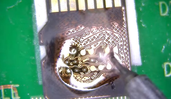
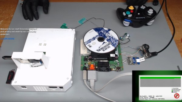
That did not stop [DeadlyFoez] from trying anyway, planning out the steps he needed to achieve a hacked Mini unit with the help of a regular Wii donor, already hacked. After dumping both systems’ NANDs and exploring the Wii Mini hardware further, he found a few pleasant surprises. There are test points on the board which allow GameCube controllers to be used with it. There are also SD card connections physically present on the board, but the support was removed from the Mini’s system software.
The most interesting parts come later on however: by simultaneously swapping NAND and GPU chips between original Wii and Wii Mini, [DeadlyFoez] manages to put together two distinct systems. The first is an original Wii board with the Mini’s chips claimed to be “the first Wii Mini running homebrew software”. The second, filling the opposite side of the equation, with both hardware and software to add SD card and GameCube controller ports to a Wii Mini.
This process of BGA rework in order to mod Nintendo hardware into unorthodox versions of themselves has actually been done before a few years ago, when someone made an unofficial US region non-XL new 3DS by piecing together parts from two separate consoles. Continue reading “Defeating The Wii Mini As The Internet Watches Over Your Shoulder”