PSP 3000 Hacked

Peripheral manufacturer Datel has been hard at work attempting to crack the PSP 3000 since its release. They’ve developed the Lite Blue Tool battery to force the PSP into service mode so hackers can run any arbitrary code they want. According to MaxConsole, Datel performed a silicon level investigation of the PSP’s chips to determine how to break into service mode. This means they decapsulated the the chips and reverse engineered any cryptographic protections. We’d love to hear exactly what chips were being used since some are fundamentally flawed.

Silicon hacking has always been a favorite topic of ours and we suggest you check out [Chris Tarnovsky]’s decapsulation technique to learn more about it.

Reverse Engineering Silicon Logic

[Karsten Nohl] has recently joined the team on Flylogic’s blog. You may remember him as part of the team that reverse engineered the crypto in MiFare RFID chips. In his first post, he starts out with the basics of identifying logic cells. By studying the specific layout of the transistors you can reproduce the actual logic functions of the chip. The end of post holds a challenge for next week (pictured above). It has 34 transistors, 3 inputs, 2 outputs, and time variant behavior. Also, check out the Silicon Zoo which catalogs individual logic cells for identification.

HOPE 2008: The Impossibility Of Hardware Obfuscation


The Last HOPE is off and running in NYC. [Karsten Nohl] started the day by presenting The (Im)possibility of Hardware Obfuscation. [Karsten] is well versed in this subject having worked on a team that the broke the MiFare crypto1 RFID chip. The algorithm used is proprietary so part of their investigation was looking directly at the hardware. As [bunnie] mentioned in his Toorcon silicon hacking talk, silicon is hard to design even before considering security, it must obey the laws of physics (everything the hardware does has to be physically built), and in the manufacturing process the chip is reverse engineered to verify it. All of these elements make it very interesting for hackers. For the MiFare crack, they shaved off layers of silicon and photographed them. Using Matlab they visually identified the various gates and looked for crypto like parts. If you’re interested in what these logic cells look like, [Karsten] has assembled The Silicon Zoo. The Zoo has pictures of standard cells like inverters, buffers, latches, flip-flops, etc. Have a look at [Chris Tarnovsky]’s work to learn about how he processes smart cards or [nico]’s guide to exposing standard chips we covered earlier in the week.

Exposing And Photographing Silicon

Have you ever wanted to break open your IC and see where those pins really go? [nico] goes through his process of dissolving ICs to their core and photographing the tiny die. The technique involves liquefying the package in sulfuric acid until all the packaging material and pins are gone. He even explains how to use sodium bicarbonate (common baking soda) to neutralize the solution thus allowing for simple sink disposal. Although silicon hacking is generally done by funded hackers with a really nice lab, it is certainly possible to execute some of these techniques with limited equipment and chemical access. For instance, if you can’t get sulfuric acid, send your IC off to a failure analysis lab like MEFAS. For more information and stories on silicon hacking, check out [Chris Tarnovsky]’s process for hacking smartcards and [bunnie]’s talk Hacking silicon: secrets behind the epoxy curtain.

Silicon Hacking


Wired recently posted an article and video detailing our friend [Chris Tarnovsky]’s process for hacking smart cards. In the video, [Chris] shows how he strips away physical components of the chips inside the smartcards using various gadgets and chemicals.

The first step is to remove the chip from its plastic frame. After soaking it in acid for about 10 minutes, the epoxy is removed and the chip is exposed. After that the outer layer is loosened by soaking the chip in two solutions of acetone, the second being the “clean” one. Then the chip is placed on a hotplate where a drop of fuming nitric acid is applied with a dropper; the chip is washed again in an ultrasonic cleaner, removing any residue left.

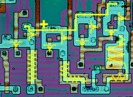
[Chris] then returns the chip to the card. He will apply nail polish to act as a masking material. He scratches a hole through the polish with a needle held by a micro positioner in the area of interest. The hole is treated with hydrofluoric acid and then etched in short intervals until the desired layer of silicon is exposed. At this point, the card is fully prepped.

Now by powering the chip with the needle resting on the bus, [Chris] can read the code on the chip by sending it various commands and watching how it reacts. To see more of [Chris]’s reverse engineering work, check out Flylogic Engineering’s Analytical Blog. It’s a enjoyable read even if you’re new to silicon hacking.

DISH Wins $1050 In Satellite Cracking Case

Who doesn’t love a good corporate espionage story? We certainly don’t mind them, especially when they involve hiring a notable hacker to do the company’s dirty work. It seems this is exactly what happened in the case of Dish Networks vs NDS Group. Last month, Christopher Tarnovsky admitted he was paid $20,000 in cash to crack the security protocols used on DISH Network access cards. NDS Group claimed the reverse engineering was simply for comparative reasons while DISH is said it resulted in $900 million in damages.

The trial came to an end this week with the court finding NDS group guilty of cracking 1 card (a fine of $49.69) and liable for an additional $1000 in damages. Not quite the big payoff DISH was hoping for, but both companies have expressed feelings of vindication about the decision. DISH Networks says that the jury ruled in their favor, proving that they were right all along (just not $900 million dollars right). NDS maintains that Tarnovsky’s work was never publicly shared and that they never intended to flood the black market with cracked cards as DISH has implied.

Make Your Own Aerogel

Our own [Eliot] dug this one up from the grave. While the recipe has been online for a while, do you know many 10 year olds who made their own Aerogel, that wonderful insulator that’s essentially gelled air? [William] made some(cache) for his science project in 2002. He started with Silbond H5, a combination of ethyl alcohol and ethyl polysilicate. You can get the MSDS after a painless email registration on the Silbond website. After the gel is formed you have to soak it in an alcohol bath to make sure all water has been removed from the structure. Then the gel is placed in a drying chamber. Liquid CO2 is forced into the chamber to displace all the alcohol in the chamber and the structure. Once the the alcohol is gone the supercritical drying phase begins. The temperature is raised to 90degF and the pressure is regulated to 1050psi. At this point the liquid CO2 in the gel structure takes on gas properties (looses surface tension) and leaves the silica structure. All that remains in the chamber is your new Aerogel which is 99% empty space and 1000 times less dense than glass.

Of course, if you’re lazy, you can buy some here.