If you’re used to working through a microscope, you’ve probably noticed that the angle of the light greatly affects how your workpiece looks. Most of us prefer the relatively flat lighting provided by a ring light, but variable angle side lighting can be useful too, especially when you’re peering inside ICs to make sure the silicon is what it’s supposed to be.
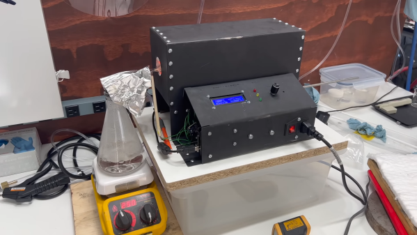
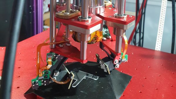
That’s what [Bunnie] is working on these days with his Project IRIS, short for “Infrared in situ,” a non-destructive method for looking inside chip packages. The technique relies on the fact that silicon is transparent to certain wavelengths of light, and that some modern IC packages expose the underside of the silicon die directly to the outside world. Initial tests indicated that the angle of the incident IR light was important to visualizing features on the metal interconnects layered onto the silicon, so [Bunnie] designed a two-axis light source for his microscope. The rig uses curved metal tracks to guide a pair of IR light sources through an arc centered on the focal point of the microscope stage. The angle of each light source relative to the stage can be controlled independently, while the whole thing can swivel around the optical axis of the microscope to control the radial angle of the lighting.
The mechanism [Bunnie] designed to accomplish all this is pretty complex. Zenith angle is controlled by a lead screw driving a connecting rod to the lights on their guide tracks, while the azimuth of the lights is controlled by a separate motor and pulley driving a custom-built coaxial bearing. The whole optical assembly is mounted on a Jubilee motion platform for XYZ control. The brief videos below show the lights being put through their paces, along with how changing the angle of the light affects the view inside a chip.
Continue reading “Adjustable Lights Help Peer Inside Chips With IR”