suspended carbon nanotube

Falling Down The Carbon Rabbit Hole

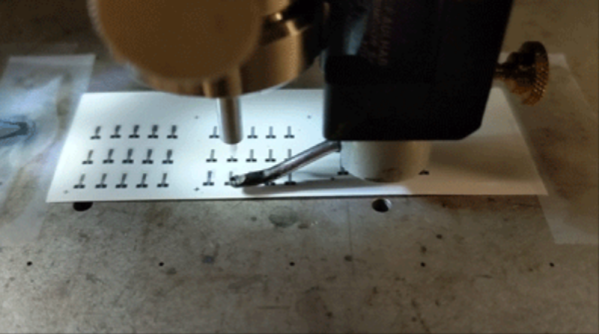
Research projects have a funny way of getting blown out of proportion by the non-experts, over-promising the often relatively small success that the dedicated folks doing the science have managed to eke out. Scaling-up cost-effectively is one of the biggest killers for commercializing research, which is why recent developments in creating carbon nanotube transistors have us hopeful.

Currently, most cutting-edge processes use FETs (Field Effect Transistors). As they’ve gotten smaller, we’ve added fins and other tricks to get around the fact that things get weird when they’re small. The industry is looking to move to GAAFETs (Gate All Around FET) as Intel and Samsung have declared their 3 nm processes (or equivalent) will use the new type of gate. As transistors have shrunk, the “off-state” leakage current has grown. GAAFETs are multi-gate devices, allowing better control of that leakage, among other things.

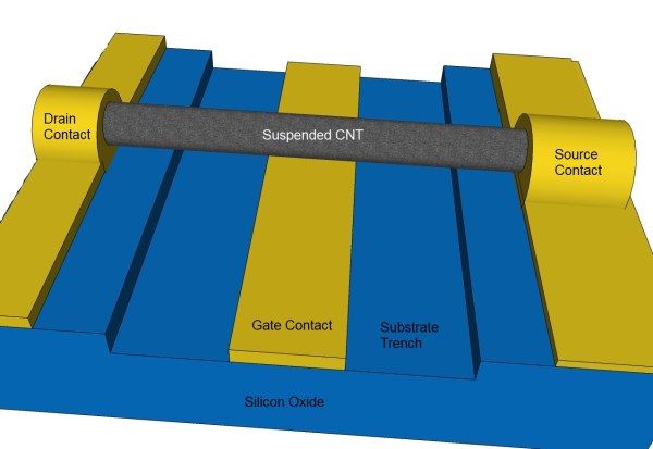
As usual, we’re already looking at what is past 3 nm towards 2 nm, and the concern is that GAAFET won’t scale past 3 nm. Carbon Nanotubes are an up-and-coming technology as they offer a few critical advantages. They conduct heat exceptionally well, exhibit higher transconductance, and conduct large amounts of power. In addition, they show higher electron mobility than conventional MOSFETs and often outperform them with less power even while being at larger sizes. This is all to say that they’re an awesome piece of tech with a few caveats. Continue reading “Falling Down The Carbon Rabbit Hole”

Miller (Effect) Time

While the Miller effect might sound like fun, it is actually the effect of parasitic capacitance in amplifiers. What do you do about it? Watch the video below the break from [All Electronics] and find out. We like how the test circuit it uses has a switch to put the mitigation circuitry in and out of the test for comparison purposes.

Actually, the Miller effect can refer to any impedance but in practice that is most often parasitic capacitance because of the construction used for tubes and transistors. The sometimes tiny capacitance gets multiplied by the inverting gain of the stage and increases the amplifier’s input impedance. This, in turn, reduces the bandwidth of the stage.

Continue reading “Miller (Effect) Time”

An Explanation Of A Classic Semiconductor Riddle

Back in 1996, Bob Pease posed an experiment in an April Fools column. “Take an ordinary NPN transistor, ground the base, pull the emitter up to 12 V with a 1 KΩ resistor and measure the collector voltage referenced to ground.” Do the experiment, and you might be surprised to find a small negative voltage present on the collector. [Filip Piorski] has always loved the riddle, and has explained how it works in a Youtube video.

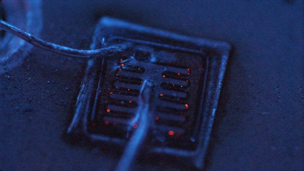
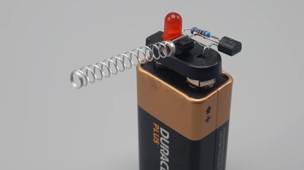
The key to the trick is the breakdown voltage of the transistor; normally somewhere around 7-8 volts for a typical small NPN transistor. At this point, where the base-emitter junction enters the breakdown regime, it begins to emit light. This light actually travels through the silicon lattice, where it reaches the base-collector junction, which acts like a photodiode under the right conditions. This generates the negative voltage seen at the collector under these conditions.

[Filip] goes on to try the experiment with a TO-3 transistor with the top cut off so he could visualise the effect in action. His photos, taken in a dark room, show tiny flecks of light appearing at spots on the silicon die. If you’ve got more insight on the effect in action, drop a comment below.

It might seem like a simple curiosity, however silicon junctions and their light emissions are an area of active research in semiconductor physics. Video after the break.

Continue reading “An Explanation Of A Classic Semiconductor Riddle”

3D Printed Transistor Goes Green

We’ll be honest, we were more excited by Duke University’s announcement that they’d used carbon-based inks to 3D print a transistor than we were by their assertion that it was recyclable. Not that recyclability is a bad thing, of course. But we would imagine that any carbon ink on a paper-like substrate will fit in the same category. In this case, the team developed an ink from wood called nanocelluose.

As a material, nanocellulose is nothing new. The breakthrough was preparing it in an ink formulation. The researchers developed a method for suspending crystals of nanocellulose that can work as an insulator in the printed transistors. Using the three inks at room temperature, an inkjet-like printer can produce transistors that were functioning six months after printing.

Continue reading “3D Printed Transistor Goes Green”

The Imperfect Bipolar Transistor

We like to pretend that our circuit elements are perfect because, honestly, it makes life easier and it often doesn’t matter much in practice. For a normal design, the fact that a foot of wire has a tiny bit of resistance or that our capacitor value might be off by 10% doesn’t make much difference. One place that we really bury our heads in the sand, though, is when we use bipolar transistors as switches. A perfect switch would have 0 volts across it when it is actuated. A real switch won’t quite get there, but it will be doggone close. But a bipolar transistor in saturation won’t be really all the way on. [The Offset Volt] looks at how a bipolar transistor switches and why the voltage across it at saturation is a few tenths of a volt. You can see the video below.

To understand it, you’ll need a little bit of math and some understanding of the construction of transistors. The idea of using a transistor as a switch is that the transistor is saturated — that is, increasing base current doesn’t make much change in the collector current. While it isn’t perfect, it is good enough to switch a relay or do other common switching tasks.

Continue reading “The Imperfect Bipolar Transistor”

Retrotechtacular: Manufacturing Philco Germanium Transistors

There was a time when all major corporations maintained film production departments to crank out public relations pieces, and the electronic industry was no exception. Indeed, in the sea-change years of the mid-20th century, corporate propaganda like this look at Philco transistor manufacturing was more important than ever, as companies tried to pivot from vacuum tubes to solid-state components, and needed to build the consumer electronics markets that would power the next few decades of rapid growth.

The film below was produced in 1957, just a decade since the invention of the transistor and only a few years since Philco invented the surface-barrier transistor, the technology behind the components. It shows them being made in their “completely air-conditioned, modern plant” in Pennsylvania. The semiconductor was germanium, of course — the narrator only refers to “silly-con” transistors once near the end of the film — but the SBT process, with opposing jets of indium sulfate electrolyte being used to both etch the germanium chip and form the collector and emitter of the transistor, is a fascinating process, and these transistors were quite the advance back in the day. It’s interesting, too, to watch the casual nature of the manufacturing process — no clean rooms, no hair nets, and only a lab coat and “vacuum welcome mats” to keep things reasonably clean.

As in most such corporate productions, superlatives abound, so be prepared for quite a bit of hyperbole on the part of the Mid-Atlantic-accented narrator. And we noticed a bit of a whoopsie near the end, when he proudly intoned that Philco transistors would be aboard the “first Earth satellite.” They were used in the radio of Explorer 1, but the Russians had other ideas about who was going to be first.

And speaking of propaganda, don’t forget that at around this time, vacuum tube companies were fighting for their lives too. That’s where something like this designer’s guide to the evils of transistors came from.

Continue reading “Retrotechtacular: Manufacturing Philco Germanium Transistors”

Simple AC Current Detector Built On A 9 Volt

When working around mains voltages, it can be useful to know whether a given circuit is live or not. While this can be done by direct connection with a multimeter, non-contact methods are available too. A great example is this simple wireless AC current detector from [NEW PEW].

The circuit is a simple one, and a classic. The spring from a ballpoint pen is soldered to the base of a BC547 transistor, and when held close enough to a conductor carrying AC power, a current is induced in the spring which is sufficient to turn the transistor on. The transistor then switches on a second BC547, which lights an LED. The whole circuit is built on top of a battery clip so it can be run straight from the top of a standard 9 volt battery.

It’s a circuit you’ll find all over the place, even built into many modern multimeters. It can be particularly useful to help avoid drilling through mains wires embedded in the walls of your home. Of course, if you’d like even more information about what’s lurking within your walls, consider this capacitive imaging hack. Video after the break.

Continue reading “Simple AC Current Detector Built On A 9 Volt”