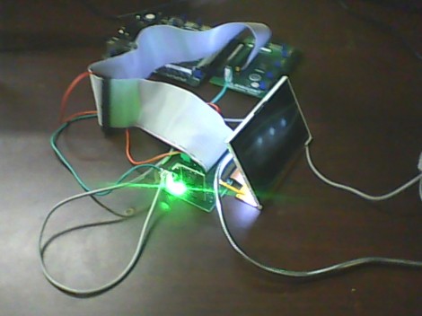
[Cesar] recently got a PSP display up and running with his FPGA development board. That’s a nice project, but what we really like is that he set aside a lot of time to show how it’s done every step of the way. This isn’t just a tutorial on that particular screen, but an overview of the skill set needed to get any piece of hardware working.
The screen itself is a Sharp LQ043T3DX02; a 480×272 TFT display with 16 million colors. Not bad for your project but when you start looking into the control scheme this isn’t going to be like using a Nokia screen with an Arduino. It takes twenty pins to control it; Red, green, and blue take sixteen pins, four pins are used for control, the rest are CK, DISP, Hsync, Vsync.
Wisely, [Cesar] designs his own interface board which includes the connector for the ribbon cable. It also has drivers for the screen’s backlight and supplies power to the device. With hardware setup complete he digs into the datasheets. We just love it that he details how to get the information you’re looking for out of this document, and shows his method of turning that first into a flow chart and then into code for the FPGA.


16 pins for RGB, +
4 for control, +
4 for CK, DISP, Hsync, Vsync =
20 pins?
I hope that this does not constitute hijacking a thread. What would be invaluable is an FPGA programmed to do the exact inverse of what is presented here. There are surely hundreds of people like me who desperately wish to scrape data off of an LCD without designing one-off hardware to do the chore. ‘Any experienced FPGA jockey out there up to the task?
Bob, just as that would require one off hardware it’d need a one of fpga design. But it’d be, should be that is, very easy to do.
Ren, maybe the 4 control pins are CK, DSP, HS and VS? They do control the screen after all.
In many ways I think interfacing hardware with FPGAs is easier than bitbanging once you grok them. It’s just that few people are more familiar with HDLs than other programming languages by the time they get their hands on a PLD.
Ren’s point is that 16 + 4 + 4 = 24 pins, not 20.
I assume that “scrape data off an LCD” means reading data off the bus to reconstruct what’s being shown. Alex is right, you’d need custom programming for most cases.
You could probably develop an FPGA scraper for a few common LCD controller chips, but it wouldn’t be universal.
Someone might also be able to program an FPGA to analyze the bus data and reverse-engineer the unknown protocol + timing, but it’s not going to be me.
I meant maybe he counted the 4 control pins twice as in 16 RGB + 4 control pins (i.e. DSP, CLK, HS, VS)
Also, HAD guys I accidently clicked the report comment button when I meant reply! Sorry :)
People have been trying for years to get these screens (PSP screens) working without buying a super expensive controller board for it (~$100 for the controller alone)… Glad to see someone making progress at the very least.
Good job for displaying a static image with this project.
I am currently looking at building something similar, but needed the image to be animated which requires updating the frame buffer. From what I can tell, the onboard RAM is being used as a single port frame buffer. If you want to change the image stored in RAM, you’d need a second RAM port connected to a micro/softcore processor.
Has any development gone into this or can anyone suggest a similar hardware IC that can handle the PSP pixel resolution? Microchip makes a PIC24 that can handle QVGA, but that only has 96Kb frame buffer data.
Thanks
Here are a few links that should help get you started, including driver boards, AVRs and micro controllers used:
http://www.lcdinfo.com/products/usbd480-lq043.html
http://www.avrfreaks.net/index.php?name=PNphpBB2&file=viewtopic&t=62356
http://www.recontech.co.uk/
This one is translated:
http://babelfish.yahoo.com/translate_url?doit=done&tt=url&intl=1&fr=bf-home&trurl=http%3A%2F%2Fwww.elektronik-projekt.de%2Fthread.php%3Fpostid%3D58469&lp=de_en&btnTrUrl=Translate
PVanecek, check this: http://www.lcdinfo.com/products/usbd480-lq043.html
Nice job. The data lines look similar to a VGA signal except with the extra clock and display pins, and the RGB are in parallel 565 mode digital lines instead of analogue. I bet it wouldn’t take too much to modify the PSP display output lines to output to DVI or VGA displays.
I don’t know how to use Verilog or VHDL but the more I see these achievements, the more it interests me. Although, it looks difficult/long-winded to define each component correctly, not sure.
For the 9 MHz clock, couldn’t he just multiply 50 MHz by 45 and divide by 250 to get 9 instead? Maybe I misunderstood?