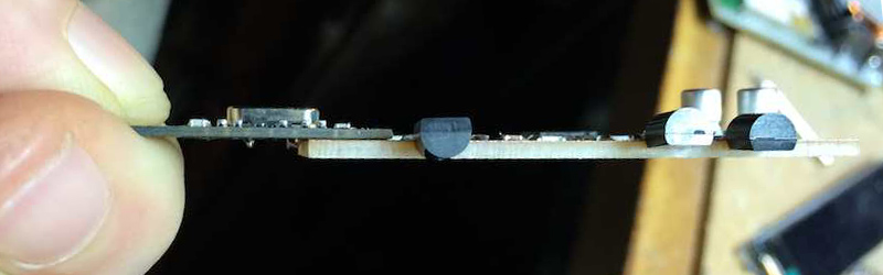
[Howard Matthews] mills his own PCBs, and man, does he hate drilling through-holes. Manually changing the bits between engraving and drilling after isolation routing? What is this? The stone age? [Howard] decided to rethink his DIY PCB manufacturing process, and came to one essential conclusion: Only a fraction of these drills are actually necessary.
Many of our cheap and beloved components, such as the NRF24L01+ and ESP-01 wireless modules come with unnecessarily bulky pin headers. To get away without drilling, [Howard] figured, that all he needs to do is leave out the pin headers and mount these modules board-to-board, using what could be best described as a BGA (blob grid array).
To mount an NRF24L01+ module, [Howard] first removes the pin headers from the module and cleans the pads. He then tins the eight corresponding pads on his milled PCB and adds two index blobs. Kapton tape surrounding the joint helps with the isolation. The module’s plated holes are then first soldered to these index blobs before the other holes are filled with solder to make a connection.


The result is pretty slick, since board-to-board mounting saves a lot of space, although the pin-header-removal step undermines the productivity aspect of the trick. Modules with castellated mounting holes are still slightly more expensive and not always available, so this might be a nice technique to keep in mind. Got some even better pro-tips on DIY PCB manufacturing? Put them right below in the comments!


I more like the way of hanging 2N2222s off the side so you can pressure clamp them against a heatsink and run 5 amps through them >:-D
Long Long Ago and far far away we epoxied a 2N2222 into the side of an aluminum cup such that the epoxy part was inside and the leads were on the outside. Fill cup with water, transistor will take many many amps as it bubbles merrily away at 100˚C. At least until the steam bubble gets big enough to let the transistor overtemp and/or the leads get hot enough to melt something.
Putting the transistor in an active water flow gets you a few more amps. Eventually something melts however.
Interesting….
I have some 2 Ohm wire-wound resistors on long leads that I use for various kinds of load testing. When they get too hot, I often chuck them in a bucket of water. The leads go a bit rusty and the solder reacts with with the whatever the water and contamination molecules get split in, but otherwise works well for very high amps, and much quieter than and cheaper than heat-sinks and fans.
Why have I been drilling holes for transistors when I could have been using this trick. Excellent find!
You don’t have a three pronged transistor bit ? ;-)
I tried this with a Pro Mini board in my Tote robot, and I don’t recommend it — a lot of problems with unreliable connections, no way to actually inspect the connections, very hard to desolder the board.
I found it’s much easier to have holes in the other board too, large enough to put your solder wire through it — then you just melt it on both ends — guaranteed good connection.
Hmm, yeah, sounds like a really clever idea. Replacing the work of changing a drill bit with this complicated error prone process…
I’m too lazy to change bits… so I’ve been known to use the drill press, the hand drill press stand and a handheld electric drill, with different size bits in… I somehow collect too many handheld drills… buy a tool cabinet, free drill, oh okay, now I can go to 5 bits/implements at once….
I totally agree, Steve. A CNC milled board is the one time when CNC drilling the holes is easy and accurate. Much quicker than this. Not to mention the risk of lifting pads if there’s any pressure on the daughter board.
I got frustrated CNC drilling holes in a board that I’d photo etched, but that was due to alignment/scaling problems.
As Howard Matthews says at the bottom of his blog page “Note: this is a hacky and, arguably, utterly unnecessary technique, but I like it, so there ????”
‘Nuff said.
“Just. Can’t. Be. Arsed.” my foot! Of course it’s ridiculously inefficient and produces a result that you wouldn’t want to put into any kind of production or even many prototypes. This was done just because he could, and wanted to see what would happen next – the tinkering/hacking/experimentalist imperative.
I did one a while back. Loads of pogo pins. Like anew upsidedown pyramid. You conect it it via boards breaking it out into a cube. A box on the outside keeps the chip locked on top. So it’s a bit like a headphone jack on steroids. I wish they were commercially available.
I remember doing this with my RPi bluetooth adapter. I even used only solder to do the necessary ‘wirings’.
I would do this if only the drill press was not working. It would be awful lot of work to fix if any two pads got shorted during soldering.
Can you not just flux the main pcb, and then just blob the solder into the through-hole while holding them in place?
This is just castellated mounting where the castellation is 360 degrees. Not even a hack.
Hey, or you could use a flux capacitor to keep a steady level of flux throughout the process! :-D
Shit, now I’m going to have to put my flux in a syringe and slide the wrap off a large electrolytic and reshrink it on there, just to mess with people.
Don’t use syringes, use an artists water brush pen, a lot easier to use and you can carry your toolbox into a drug neighborhood without getting arrested
+10 ROFL
I like this idea. Tried it myself a while ago. Works only if the boards have real through hole plating.
Now, speaking of headers, anyone know an easy way to remove those headers from the nucleo boards?
If those are standard .1″ header pins (don’t know that nucleo board), you could just push a high-ish wattage iron to the not-soldered side until both the plastic and the solder melt, and push it through. works for me
One pin at a time.
i have done this a few times out of pure laziness xD
Ever since I owned a drill press and used a head steapped magnifier I can drill pretty accurately and without breaking drill bits. I do prefer smd now that I own a rework station though, so I try to keep through hole to a minimum. Having good lighting on the board helps a great deal. I use a swan necked led lamp that can be easily positioned. It only takes about 15 mins to drilk most small pcbs I make. Designing in eagle takes the most time. Developing a board about a couple of hours.
Etching with 30% hcl and 10% h2o2 takes about 10 mins, using the redulting cucl solution about 20mins. I do reuse it and just add a bit of h2o2 to reactivate the acid and heat it up by putting the small acid container in a large tank with hot tap water. Do it outside or near an open window. It does sting a bit in the nose and eyes.
I’ve been planning on doing this with the Pi Zero. I’ve got a footprint that leverages all of the USB pads and the test points. Because it ships without headers, I don’t have to remove them, making it easier. It also keeps the whole project low profile. However, should something fry, this is going to be a pain and a half to try and troubleshoot.
You do need a module with a completely flat bottom side. The Pi Zero still requires two holes, one each for the leads of the connector that comes through the board.
Here’s how much I hate drilling holes –
https://cdn.hackaday.io/images/4747701466897513322.jpg
https://cdn.hackaday.io/images/6161931471394932892.jpg
+1
That’s pretty unholey.