
We’ve previously remarked upon a generation lucky enough to be well-versed in microcontrollers and computersised electronics through being brought up on the Arduino or the Raspberry Pi but unlucky enough to have missed out on basic electronics such as how to bias a transistor, and to address that gap we’ve taken a look at the basics of transistor biasing.
All the circuits we worked with in the previous article had the transistor’s emitter taken to ground, took their input from the base, and their output from the collector. This configuration, called a Common Emitter amplifier is probably the most common, but it is far from the only way to use a transistor. Once you have set up the bias voltage as we described to the point at which the transistor is in its linear region, there are several other ways in which the device can be used as an amplifier. The subject of this article is one of these configurations, so described because it takes the transistor’s base to the ground instead of the emitter, as a Common Base amplifier.
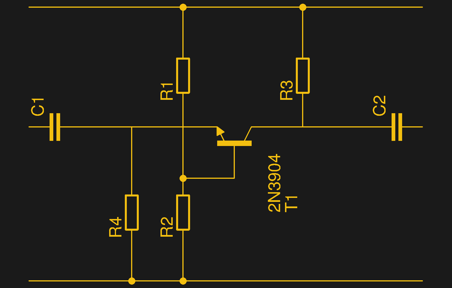
Take a moment to consider the most basic common base amplifier. The transistor’s base is held at a constant bias potential, its emitter forms the amplifier’s input, and the collector its output. The DC biasing arrangement is exactly the same as the common emitter amplifier we have previously described, in that the base is held sufficiently higher than the emitter that the transistor is conducting in its linear region, and there is an emitter resistor to limit the current through the device. The emitter circuit has a small load in it across which the input is placed, and the output comes from the collector as with he common emitter circuit.
When the voltage at the emitter is varied by changing the amplifier input, it in turn varies the voltage between base and emitter. As the voltage between base and emitter varies, so does the base current, which in turn causes a much larger variation in the collector current due to the transistor’s gain. This causes a correspondingly larger voltage variation across the collector resistor which is available at the output as an amplified version of the smaller signal on the emitter.
There are two consequences of this mode of operation that give the common base amplifier significantly different properties to its common emitter siblings. It is a voltage amplifier rather than a current amplifier, it is non-inverting, and it has an extremely low impedance at its input.
When we examined the common emitter circuit we took a look at the fundamental of how a transistor works, that the current flowing through its collector is a multiple of that through its base, that multiple being referred to as its gain. Thus on changing the base current we generate a correspondingly larger change in the collector current from which we can derive an amplified voltage across a collector resistor, but we will always require our input to be a source of current rather than of voltage. By comparison with the common-base circuit the base current comes from the bias network rather than the input, so the input can be much more like a voltage source than a current source, and thus the common base circuit is a voltage amplifier.
The common emitter amplifier that we saw last time is an inverting amplifier, in that as an increasing current on the base causes more collector current to flow it pulls the collector voltage down. Thus a voltage rise on the input causes a corresponding voltage fall on the output, and a cyclical waveform such as a sine wave is inverted by its passage through it. The common base amplifier, on the other hand, reacts to an increased voltage on the emitter, its input, by drawing less current, and the voltage left over on the output increases.
Finally, the input impedance of a common base amplifier is significantly lower than its common-emitter equivalent. The collector circuit of a transistor amplifier can either be a very low resistance or a reactive circuit with a zero resistance DC path. By comparison the impedance of the base circuit on the common emitter amplifier with its resistor network is much higher. In most cases the high impedance of a common emitter amplifier input is a huge advantage over the low impedance of the common base configuration because it does not load the circuit from which it derives its input, but in cases where an impedance match is required with a low impedance source, the common base amplifier’s low impedance becomes an advantage. Thus you will find common base amplifiers used in small-signal RF amplifiers where a match with a low-impedance feeder, and in amplifiers for low-impedance audio sources such as moving-coil microphones. The antenna preamplifier in an analog TV tuner was frequently a common-base design for this reason.
You may never build a common-base amplifier unless you work with RF, but it remains a useful configuration to know about and a handy weapon in your arsenal of circuits for when you need a voltage amplifier with a low impedance input. We will continue this series by looking at the final configuration for a transistor amplifier, the common collector amplifier or emitter follower, before examining the equivalent circuits using field effect transistor, or FET.


Dots good!
B^)
(said with an old Cherman accent)
But it would be das goot in the Germans from Russia Ellis County dialect(s) I grew up with.
With the schematic it would help if the supply rails had Vcc and gnd attached to it. Also to add a dot when lines connect vs cross.
oh I missed that one dot. Still, when three lines come together I usually add a dot too, for clarity.
I think Jenny read the comments in the previous transistor article.
I’m not sure what you mean to say.
I mean there was a long comment thread about putting dots at crossings (as well as T joints and stuff).
The schematic seems to be missing a bypass capacitor for the base. The way it is drawn, base has nowhere near constant voltage and input impedance is also quite high.
Speaking of capacitors, a former classmate noticed that the capacitance values for coupling capacitors were much higher than capacitors doing the same function in vacuum tube (valve -Jenny) circuits.
Makes sense for BJT circuits, because bipolar transistor base takes much more current than a vacuum tube grid. Closer equivalent would be FET circuits, which don’t need as big coupling caps.
It’s an ideal circuit for demonstration purposes. Hence also no resistor values.
What are the relative benefits of using a transistor as an amplifier vs. an op amp (aside from the obvious that a transistor costs less)?
> it remains a useful configuration to know about and a handy weapon in your arsenal of circuits for when you need a voltage amplifier with a low impedance input.
Aside from the cost, transistors can be selected over much wider set of operating conditions. Need 2.4 GHz amplifier? Easy to find such a transistor, good luck finding such opamp. Need output power of 10 Watts? Much easier to find a high-power transistor (you could of course use an opamp to drive it, though).
Often speed. Often impedances that are awkward to achieve with a general purpose op-amp at high frequencies. Simplicity in many applications.
What do you think op amps are made of? :P
They(op amps) contain capacitors, resistors, and transistors of course. However that’s irrelevant when an op amp to fit your needs isn’t being manufactured.
The linked UHF tuner article made me want to experiment more with RF.
“As the voltage between base and emitter varies, so does the base current, which in turn causes a much larger variation in the collector current due to the transistor’s gain.”
Danger Will Robinson!
“This causes a correspondingly larger voltage variation across the collector resistor which is available at the output as an amplified version of the smaller signal on the emitter.”
KaBooom. *flaming tyre rolls out*
The gain cannot automatically be beta, because the collector current and emitter current are (essentially) the same.
I built one of these at university because it just didn’t look like an amplifier to me. I need to dust some cobwebs from some dark corners but I think R3 being higher than R4 is a requirement for amplification.
Me before readying the article: “I may not have an EE degree but I know enough to be dangerous with basic transistor amplifiers”.
Me after reading: “…” (quietly walks off stage)
Most of my work with common-base stages was using them as the output of a cascode with a common-emitter input stage.
This let you eliminate most of the Miller capacity effect on the input, and go faster at high output swings, as in CRT cathode drivers “back in the day”. Then, most transistors that would do high voltages had terrible Hfe – so the common emitter input id the current gain and biased the HV-but-otherwise-crappy output transistor. And yes, of course you bypassed the common base.
I’ve also used the common base as the gain part of RF oscillators.
Hi Doug, you won’t know me but I recognise you from the fusor crowd:)
R1 and R2 are throwing me, they don’t seem to make sense for a capacitively coupled common base amplifier, since it’s biased by bootstrap if the base is grounded and there is no need to set the emitter or collector voltage with it capacitively coupled. Any thoughts?
If the base were at DC ground, the emitter would need some current from a negative rail (to mostly wind up at the collector and pull it off the positive rail). I think what they were intending here is that the bottom rail is DC (and also AC) ground, while the base is only AC ground, as it obviously has to be biased somewhat above the turn-on volts compared to the emitter to work at all (that .6 or .7v thing). Hence, those R’s are used to split the DC supply up. If the Hfe is super high and the R’s small, you might not notice the loss of gain from no bypass as the base wouldn’t move around that much (by the time the input signal is affecting the base current *bigtime* we’ve been deep in clipping anyway). And yes, to have voltage gain (as we know we won’t have current gain here), the collector resistor has to be larger than the emitter one (we could use “impedance” instead and still mean the same thing).
This circuit was drawn kinda sideways compared to what I’d have done for easy understanding. If you did the conventional emitter at the bottom and collector at the top orientation, it’s obvious you need to pull the base up off ground to get some volts across the emitter resistor so you have some DC drop at idle and won’t clip with zero signal.
“The common base amplifier, on the other hand, reacts to an increased voltage on the collector, its input, … .” Wait, I thought the emitter was the input.
You are correct.
… and now so is the article.
(That was my bad, not Jenny’s, BTW. I always get them confused. Anyone have a good mnemonic? That works with PNP transistors as well?)
As dcfusor2015 mentioned, miller capacitance. Basically there are capacitances between the junctions. One in particular, the base collector capacitance hurts common emitter amplifiers at high speed. In common emitter amplifiers the input and output signals are inverted, combine that with base collector capacitance that couple them, and you are not going to have good high speed performance, With common base amplifiers, the base emitter capacitance is of almost no effect as there is no real voltage variation, only current variation. The base collector capacitance does have an attenuating effect,but at least it does so as an simple load, it does not drive an amplified, inverted signal from the output right back into the sensitive input.
Yeah, I thought that was the primary advantage of common base amplifiers (lower transistor capacitance, hence easier to use with high frequencies), but it is not mentioned at all in the article.
Most common usage…. on frequency counter inputs.
I made my first common base amplifier as a teenager messing around with audio. Not having a decent microphone I had experimented with a carbon mic from an old phone, and with a small speaker. The speaker wasn’t any use [might have been if I’d had a transformer to match 8 ohms into something I could use on a common emitter input], until I put together a common base pre-amp stage. I think it had around unity gain but wow, it sure did a good job of making that little speaker into a decent microphone.