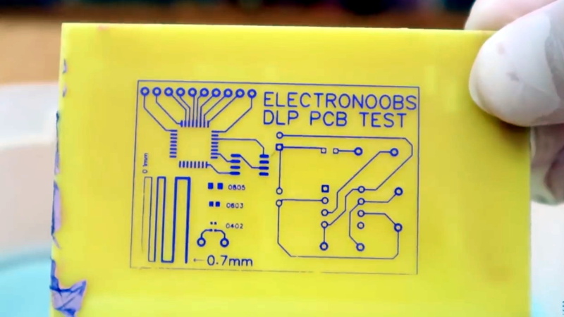
Now that these DLP printers are cheaper and more widely available, we’re starting to see hackers poking around the edge of the envelope to see what else the machines are capable of. [Electronoobs] recently got his hands on a couple of these printers, and thought he would do some experiments with using them for PCB production.
 Rather than extruding molten plastic, these printers use light to cure resin layer-by-layer. In theory if the printer is good enough to cure the light-activated resin for a high resolution print, it should be able to do much the same thing with photosensitive PCBs.
Unfortunately, getting an STL out of a PCB design program takes a few intermediary steps. In the video after the break, [Electronoobs] shows his workflow that takes his design from EasyADA and turning it into a three dimensional object the DLP printer will understand. He does this with Blender and it looks pretty straightforward, but in the past we’ve seen people do similar tricks with Inkscape if that’s more your style.
Once you’ve grafted another dimension onto your PCB design, you may need to scale it to the appropriate size. [Electronoobs] notes that his STL for a 60 mm wide PCB came out of Blender as less than 2 mm wide, so you might need to break out the dreaded mathematics to find the appropriate scale value. Once the dimensions look good, you can load this file up into the printer as you would any normal print.
On the printer side of things, [Electronoobs] manually laminates UV photoresist film onto some copper clad boards with an iron, but you could skip this step and buy pre-sensitized boards as well. In any event, you drop the board where the UV resin normally goes, press the print button, and wait about ten minutes. That should give it enough time to expose the board, and you then proceed with the normal washing and acid bath process that hackers have been doing since time immemorial.
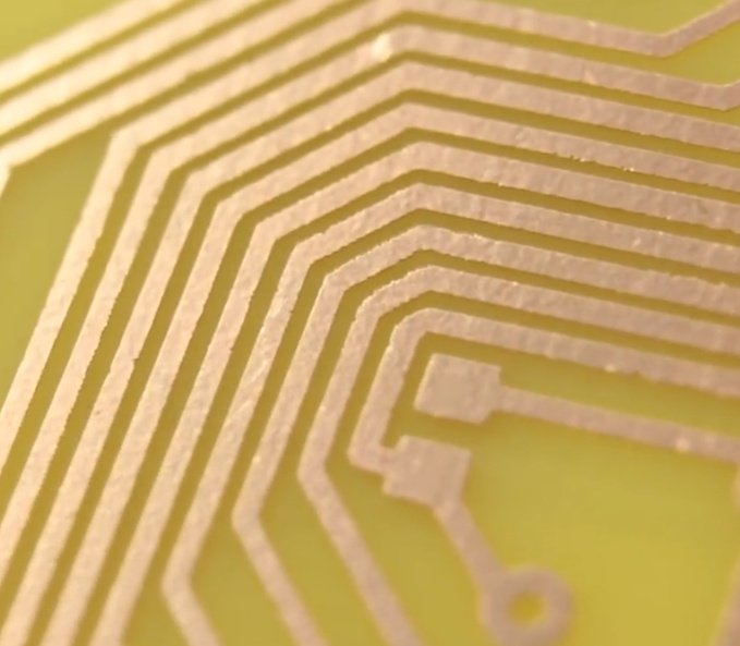
As [Electronoobs] shows, the results are quite impressive. While this still won’t make it any easier for you to do double-sided PCBs in the home lab, it looks like a very compelling method for producing even SMD boards with relative ease. This isn’t the first time somebody has tried using a DLP printer to run off some PCBs, but now that the technology has matured a bit it looks like it’s finally becoming practical.


Bit of a pet peeve of mine: Both of these machines are LCD SLA printers, not DLP printers.
DLP is a technology developed by TI that uses micromirrors to project light onto a surface. There is no DMD (digital micromirror device) in the printers, so they are not DLP devices. Instead, they have a regular LCD panel that is mounted as close to the vat as possible.
SLA (stereolithography apparatus) is a 3D printing technology that uses light to cure liquid photopolymers. To selectively cure each layer, the three technologies used today (or at least that I know of) are laser scanning, DLP and LCD.
If it’s an LCD and a UV light below, why not just load the PCB directly layout to the LCD?
https://www.3ders.org/images2016/lcd-led-based-utopiaprinter-widens-the-door-to-low-cost-diy-sla-3d-printing-3.jpg
I was thinking that too.
Yup.
https://hackaday.com/2017/10/16/why-not-expose-your-pcbs-through-an-lcd/
If you already have an SLA loafing about at your disposal, why not. But taking this path from scratch would be silly, like hammering a nail with a light gas gun. Or something.
I have no idea why some people call LCD displays DLP. If you were manipulating light with a mirror, theoretically you could get much higher resolution than by using LCD, which are raster devices and are in that sense strictly limited to their native resolution. But that’s talking about an analogue macromirror like a galvo (or the coils of a vector-style crt?) instead of digital micromirrors.
You may want to check DLP again.
LCD : Huge divergent UV source (LED or anything else) hits a LCD screen which let pass the light or not according to the pattern displayed.
Pro : “Flash” the whole active area.
Con : LCD life decay faster with UV light, resolution is fixed by your LCD
Laser Scanning : A single straight UV source (from a laser) hits a galvanometer which redirect the beam “where you want”.
Pro : Lot of power, can do vector tracing
Con : Slow, somewhat painful to caliber, it will be out of focus by design in some area, choose wisely which.
DLP : Huge somewhat divergent UV source (LED or anything else) hits an array or micro-mirrors. You can control the angle of the mirror, but most of the time, it’s just full left or full right (meaning reflecting you image somewhere, and the negative somewhere else).
Pro : “Flash” the whole active area. More power is transferred versus LCD.
Con : Delicate mechanical component (more fragile than Laser scanning), most of the time, array is “diamonslike” and not square, high price and hard to obtain datasheet.
Hope this will help.
Exactly. And if you go to the effort of carefully aligning two LCDs just once it should be possible to do double sided boards in one go.
Heck, you could probably just align it decently and then software calibrate it.
Hate to be the bearer of bad news, but SLA printers did at least at one point use DLP’s. It’s at the 4:30 mark… https://youtu.be/97ARLiTHjX0?t=270
So? Did you read all of my comment? It’s not news but a fact, that there are some DLP SLA printers (as stated in my comment). Also, I own one, so I am definitely aware of – and not shocked by – their existance. However, that still does not make the printers in the article DLP.
Fair enough, I misinterpreted your last sentence. Have your internet point back. ;) (+1)
I use to think the same. This is just the same name but in the 3D printers world it means just Digital Light Processing. It has nothing to do with the beamer and mirrors tech. I don’t like it but we have to live with that. It’s frustrating me in the same way as the bio food or organic. Other food is synthetic? But I’m not normal ;-)
Nice job, but some laborious. It is like a modern version of “old days pcb making”, pcb with KPR, exposing pcb under UV…
Shouldn’t be that hard to do double sided. Apply photoresist to both sides, use a jig for precise registration, expose both sides with correct mask and Bob’s your uncle?
Why make an STL? Surely the LCD screen would be just as happy to display a JPG?
I wrote a slicer as an Autodesk Inventor macro that outputs a multi layer SVG file, one layer per slice for a friends home-brew printer based on a presentation projector.
It seems to me that an almost-unmodified projector with the filter wheel removed would be a simpler way to do this than forcing a printer to fit?
I personally would avoide jpg due to its inherent tendency to leave noisy artifacts.
While PNG and BMP doesn’t have such artifacts.
Even if these artifacts wouldn’t be an issue, I rather be safe then sorry when it comes to such details.
Aye, I was being a bit flippant with JPG, that’s why my own DLP slicer used SVG, which keeps curves as curves, avoiding the faceting that STL introduces.
Converting to STL lets him use the regular printer software.
While I am still printing flat PCB’s, I think I will stay with the Toner Transfer method. Less time, less effort, less chemicals, same quality.
But this definitely would have some advantages when we mode to formed 3D PCB’s.
Wasn’t this done long time ago with the OpenFL of the form 1 ?
https://forum.formlabs.com/uploads/default/original/2X/c/cef113cacabfe4e072511c28311fa7a1786e9a67.png
The Photonsters group in GitHub have a software for that to use with Anycubic’s Photon.
https://github.com/Photonsters
Photoresist is less sensitive to visible light, but still a little bit sensitive. Has anybody tried opening design on a phone and leaving the pcb on it for a while? Without removing the extra glass it would be blurry, but at least as a proof of concept?
I tried with regular smarthone’s LCD, it not works. Not tried with OLED screen yet.
What about replacing the WLED backlight found in common LCD displays with UV LED backlight? That might do the trick.
Yes, I ordered some small uv leds for this, will try it later, but i mean it’s good to have parallel shadows. Flat LCD can have problems with it
Working with Photoresist annoyed me always quite a bit. First the light exposure, then the development process… lots of extra steps that require extra work and might screw up things.
I am wondering… why not use the bare copper PCB as a build platform and 3D-print the traces with a height of maybe 0.5mm onto the copper? Then just throw that into the etching solution and hope that the 3D-printed traces will mask off the copper. Would be much easier :)
I never worked with a resin printer. Any comments on that idea from someone who used such a printer? Doable or bullshit?
How different is a DLP printer from a more common video projector if you’re only using the imaging part?
Hmm, a quick search yields: https://hackaday.com/2016/01/07/make-pcbs-with-dlp-omg/
Isn’t really that different. Optics and designed to pass UV?
Furthermore, if you have some sort of alignment features, could you throw the board back in after etching, and cure some resin onto it as solder-mask?
There’s UV-curable solder mask, y’all. This might finally be the route to homemade PCBs with a mask layer without a billion intermediate steps.
That’s a really good point. Here’s something to try next and distinguish this from just placing copper clad on top of an old LCD from your monitor circa 2009 that’s still sitting around in the garage for some reason.
i really don’t see a benefit for this technique. can someone enlighten me of the advantage this offers over the standard toner method(iron-on, or uv transfer)? because it just seems to add steps so a new machine can be used, with not as fine line definition.
boy how I wish that person chose a different internet handle. :(
Aw man! Well, at least you’ve got it on Hackaday…
would it be possible to print a thin layer of resin directly onto the copper, using it as an etching mask?
Do i have to google a bloody acronym again?! ever man and their dog seems to know what “DLP” is but Me!
apparently…
But why not? It’s how you learn new things
Considering that we can get some replacement lcds for cheap I think it would make a great project to put this together and build a pcb exposure box on the cheap, has anyone tried reverse engineering the communication to display an image on the lcd ?
I’d love to work on this project so if anyone is interested please give a heads up and maybe we can team up.
But old LCDs limit you to 96DPI which is not very high resolution. 4k displays might be better. The laser printed mask (UV film with vellum printed mask, not toner transfer) can start at 600dpi. I use a 1200dpi printer and can get 0.250mm traces with consistency. So the answer as to why is it would save printing on vellum, aligning etc. Just place PCB in jig on LCD, expose, flip, expose and etch. Consistency and least steps is the key to achieving production quality.