Tiny Art Etched Into Silicon Wafers With Electron Beam Lithography

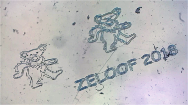
Looks like [Sam Zeloof] got bored on his Thanksgiving break, and things got a little weird in his garage. Of course when your garage contains a scanning electron microscope, the definition of weird can include experimenting with electron-beam lithography, resulting in tiny images etched into silicon.

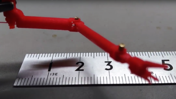
You’ll probably remember [Sam] from his 2018 Hackaday Superconference talk on his DIY semiconductor fab lab, which he used to create a real integrated circuit. That chip, a PMOS dual-channel differential amp, was produced by photolithography using a modified DLP projector. Photolithography imposes limits to how small a feature can be created on silicon, based on the wavelength of light.

[Sam] is now looking into using the electron beam of his SEM as a sort of CNC laser engraver to produce much finer features. The process involves spin-coating silicon wafers with SU-8, an epoxy photoresist normally used with UV light but that also turns out to be sensitive to electron beams. He had to modify his SEM to control the X- and Y-axis deflection with a 12-bit DAC and provide a custom beam blanker. With a coated wafer in the vacuum chamber, standard laser engraving software generates the G-code to trace his test images on the resist. A very quick dip in acetone develops the exposed chip.

[Sam] says these first test images are not too dainty; the bears are about 2.5 mm high, and the line width is about 10 μm. His system is currently capable of resolving down to 100 nm, while commercial electron beam lithography can get down to 5 nm or so. He says that adding a Faraday cage to the setup might help him get there. Sounds like a project for Christmas break.

Continue reading “Tiny Art Etched Into Silicon Wafers With Electron Beam Lithography”

Of Roach Killer And Rust Remover: Sam Zeloof’s Garage-Made Chips

A normal life in hacking, if there is such a thing, seems to follow a predictable trajectory, at least in terms of the physical space it occupies. We generally start small, working on a few simple projects on the kitchen table, or if we start young enough, perhaps on a desk in our childhood bedroom. Time passes, our skills increase, and with them the need for space. Soon we’re claiming an unused room or a corner of the basement. Skills build on skills, gear accumulates, and before you know it, the garage is no longer a place for cars but a place for pushing back the darkness of our own ignorance and expanding our horizons into parts unknown.

It appears that Sam Zeloof’s annexation of the family garage occurred fairly early in life, and to a level that’s hard to comprehend. Sam seems to have caught the hacking bug early, and by the time high school rolled around, he was building out a remarkably well-equipped semiconductor fabrication lab at home. Sam has been posting his progress regularly on his own blog and on Twitter, and he dropped by the 2018 Superconference to give everyone a lesson on semiconductor physics and how he became the first hobbyist to produce an integrated circuit using lithographic processes.

Continue reading “Of Roach Killer And Rust Remover: Sam Zeloof’s Garage-Made Chips”

Books You Should Read: Designing Reality

These days, budget CNC builds are mainstream. Homebrew 3D printers and even laser cutters are old hats. Now I find myself constantly asking: “where’s it all going?” In the book, Designing Reality, Prof Neil Gershenfeld and his two brothers, Alan and Joel, team up to answer that question. In 250 pages, they forecast a future where digital fabrication tools become accessible to everyone on the planet, a planet where people now thrive in networked communities focused on learning and making.

Designing Reality asks us to look forward to the next implications of the word “digital”. On its surface, digital  means discretized, but the implications for this property are extreme. How extreme? Imagine a time where cnc-based fabrication tools are as common as laptops, where fab labs and hackerspaces are as accepted as libraries, and where cities are self-sufficient. The Gershenfelds invite us to open our eyes into a time where digital has vastly reshaped our world and will only continue to do so. Continue reading “Books You Should Read: Designing Reality”

Tiny Vacuum Chamber Arm To Help With Homemade Semiconductors

[Nixie] wants to make semiconductors at home, and that requires some unusual tools. Chief among them is a vacuum chamber to perform thin-film deposition, and true to the hacker credo his is homemade, and will soon be equipped with a tiny manipulator arm with magnetically coupled mechanical controls.

If [Nixie]’s setup looks familiar, it might be because we featured his plasma experiments a few days ago. He was a little cagey then about his goal, but he’s come clean with his desire to make his own FETs (a project that is his 2018 Hackaday Prize entry). Doing so will require not only creating stable plasmas, but also the ability to move substrates around inside the vacuum chamber. Taking inspiration from the slender and maneuverable instruments surgeons use for laparoscopic procedures, [Nixie] is working on a miniature arm that will work inside his vacuum chamber. The video below is a 3D-printed proof-of-concept model in action, and shows how the arm’s segments will be controlled by cables. What’s really interesting is that the control cables will not penetrate the vacuum chamber — they’ll be moved right through the glass wall using magnets.

We’re keen to see chips from [Nixie]’s home fab lab, but it looks like there will be a lot of cool hacks between here and there. We’ll be watching closely. Continue reading “Tiny Vacuum Chamber Arm To Help With Homemade Semiconductors”

The Fab Lab Next Door: DIY Semiconductors

You think you’ve got it going on because you can wire up some eBay modules and make some LEDs blink, or because you designed your own PCB, or maybe even because you’re an RF wizard. Then you see that someone is fabricating semiconductors at home, and you realize there’s always another mountain to climb.

We were mesmerized when we first saw [Sam Zeloof]’s awesome garage-turned-semiconductor fab lab. He says he’s only been acquiring equipment since October of 2016, but in that short time he’s built quite an impressive array of gear; a spin-coating centrifuge, furnaces, tons of lab supplies and toxic chemicals, a turbomolecular vacuum pump, and a vacuum chamber that looks like something from a CERN lab.

[Sam]’s goal is to get set up for thin-film deposition so he can make integrated circuits, but with what he has on hand he’s managed to build a few diodes, some photovoltaic cells, and a couple of MOSFETs. He’s not growing silicon crystals and making his own wafers — yet — but relies on eBay to supply his wafers. The video below is a longish intro to [Sam]’s methods, and his YouTube channel has a video tour of his fab and a few videos on making specific devices.

[Sam] credits [Jeri Ellsworth]’s DIY semiconductor efforts, which we’ve covered before, as inspiration for his fab, and we’re going to be watching to see where he takes it from here. For now, though, we’d better boost the aspiration level of our future projects.

Continue reading “The Fab Lab Next Door: DIY Semiconductors”

How To Set Up And Run A Makerspace

A bunch of people who share a large workshop and meet on a regular basis to do projects and get some input. A place where kids can learn to build robots instead of becoming robots. A little community-driven factory, or just a lair for hackers. The world needs more of these spaces, and every hackerspace, makerspace or fab lab has its very own way of making it work. Nevertheless, when and if problems and challenges show up – they are always the same – almost stereotypically, so avoid some of the pitfalls and make use of the learnings from almost a decade of makerspacing to get it just right. Let’s take a look at just what it takes to get one of these spaces up and running well.

Continue reading “How To Set Up And Run A Makerspace”

Prof Gershenfeld Speaks On Fab Labs And All-things Digital

Fab Labs have developed hand-in-hand with the all-too-familiar hackerspaces that we see today. If you’re curious to discover more about their past and future, [Prof Gershenfeld], founder of the Fab Lab, and director of MIT’s Center for Bits and Atoms brings us a fresh perspective on both these fab labs and the digital world we live in.

In a casual one-hour chat on Edge, [Prof Gershenfeld] dives deeply into the concept of digital in our world. We might consider digital to be a binarized signal, an analog waveform discretized into a 0 and 1 from which all of computer architecture is built upon today. Digital doesn’t just exist in the computing sense, however; it’s a concept that has been applied to communication, computation, and, these days: personal fabrication.

[Prof Gershenfeld’s] talk may highlight coming changes in the future, but changes are already happening today. These days, fab labs and hackerspaces serve their communities in a very special way. They take “experts-of-the-field” away from universities and isolated labs, and they scatter them all over the world. With this shift, anyone can walk through their doors and build a solid foundation in fields like embedded programming and computer aided manufacturing by striking a conversation with these local experts. In a nutshell, both spaces found a culture for development of expertise far more accessible to the world community than their university counterparts.

If you can spare the hour, put on some headphones, tune in, and resume your CAD work, PCB layout, or that Arduino library. You may discover that your work is built on a number of digital principles, and that your contributions push the rest farther along the development chain towards building something awesome.

Finally, if you’re interested in taking notes on building your own fab lab, have a look at the inventorylayout, and guidelines at the CBA website.