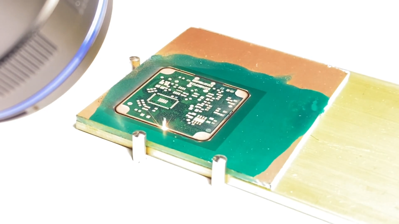
With how cheap and how fast custom PCBs have gotten, it almost doesn’t make sense to roll your own anymore, especially when you factor in the messy etching steps and the less than stellar results. That’s not the only way to create a PCB, of course, and if you happen to have access to a 20-Watt fiber laser, you can get some fantastic homemade PCBs that are hard to tell from commercial boards.
Lucikly, [Saulius Lukse] of Kurokesu fame has just such a laser on hand, and with a well-tuned toolchain and a few compromises, he’s able to turn out 0.1-mm pitch PCBs in 30 minutes. The compromises include single-sided boards and no through-holes, but that should still allow for a lot of different useful designs. The process starts with Gerbers going through FlatCAM and then getting imported into EZCAD for the laser. There’s a fair bit of manual tweaking before the laser starts burning away the copper between the traces, which took about 20 passes for 0.035-mm foil on FR4. We have to admit that watching the cutting proceed in the video below is pretty cool.
Once the traces are cut, UV-curable solder resist is applied to the whole board. After curing, the board goes back to the laser for another pass to expose the pads. A final few passes with the laser turned up to 11 cuts the finished board free. We wonder why the laser isn’t used to drill holes; we understand that vias would be hard to connect to the other side, but it seems like through-hole components could be supported. Maybe that’s where [Saulius] is headed with this eventually, since there are traces that terminate in what appears to be via pads.
Whatever the goal, these boards are really slick. We usually see lasers used to remove resist prior to traditional etching, so this is a nice change.


How is the faster and/or more efficient (energy, time, etc.) than traditional methods (mask transfer)?
Sometimes we trade speed/efficiency for the coolness factor.
having your CNC mill or Laser do it is vastly better in man hours – you spend the same amount of time plotting and laying out, then just let the machine do most of the work for you (also machines are far easier to get great double sided boards with).
Manual mask transfer, fixing the imperfections, and then etching all take supervision or active human participation.
Q: light-curable resins are a daily thing, why you no make resins that have ions handy for electrode-less metal plating?
Plated through holes are made this way: chemicals infused to the inner part of the via-hole cause metal to plate up from a bath.
If a resin could do the same trick, one could print traces, plate them up in a simple bath, and not have to burn anything away.
Additive engineering is the future…
in a DIY setting? A fair bit… the only chemical involved that needs storage is the solder mask, also the laser engraver doesn’t have any consumables whatsoever.
It’s lower effort due to minimal involvement of chemicals… photoetching is extremely messy. And this is higher quality than trasfers.
What I wouldn’t give to have this machine in my room.
Well time to rip out the laser diode from the old CD writer I guess?
CD writer diode will not help. You need pulsed energy. Actually Fiber laser machines are pretty cheap, prices start from $1.5k
Ooh. Mind linking a few?
I wish I was in a financial position where I could say $1.5k is “pretty cheap!”
Well, it’s not dirt cheap. Not long time ago price tag was about $5k and local greedy distributors charge 20k for similar spec machine. So it makes it “pretty cheap” :)
If you can settle for an intermediate step that involves chemical etching, a cheap laser engraver will work.
If a engraver laser could burn the UV soldermask, then one could use the solder mask as resist for chemical etch and burn off the reist over the pads afterward.
You can paint a PCB board and use the laser to blast off the paint, then etch as normal.
This works, although the spot size on the laser at my makerspace was too big (couldn’t make a trace that goes between two 0.1″ pads).
Looking at the Sarbar videos, it would *appear* that a well tuned CO2 laser system could etch thin enough lines for this. Getting any laser that well tuned would be a project in itself, but if you could pull it off it would be a tremendous benefit to hackers.
If you want to experiment, you can start with regular black spray paint, and bake the board to be sure all the paint is well dried.
I’m going to experiment with my SLA printer soon, since that has a lot higher resolution. Should be able to lay down a single (or small number) of layers directly on a copper board, then etch from that. SLA printers are very cheap right now.
It works for me with some help from chemistry: https://hackaday.io/project/26216-pcb-exposer
Nice results! Thank you for sharing!
Sell me a couple. One for my shop and another for my garage.
Actually you are completely wrong, you do not need a $1.5K fiber laser, you can get excellent results using a blu-ray laser diode 405nm with a 3 element lens hooked up with a good 3d/CNC printing bed frame and get excellent results, it is a lengthy process for sensitizing the photoresist and etching, some trial and error needs to be learned… this is what today’s state of the art fab-house uses today “UV-Laser” and photoresist…
But I’m on your boat and rather get a budget friendly $1.5K fiber laser, it seriously saves so much time and hassles and you will always get repeatable results using a fiber laser. I saw there are some 405nm fiber laser, planning to get that one with a telecentric lens.
Well, whole experiment was done in order to eliminate etching and mechanical processing. But glad you mentioned poor man’s solution :)
Unfortunately, it won’t be powerful enought.
Plus, you really need a fiber laser to work with metals.
Today’s advance fab house does not use a fiber laser to burn the copper off, it’s a stupid way of doing things, mainly because it’s hella expensive and inefficient. They use a UV laser near wavelength of 405nm or below to sensitize the photoresist film applied on to the FR4 copper clad and etch it out. It’s much more logical doing this way. Even the aerospace and military grade PCBs doesn’t even use fiber laser. They do however might use lasers to make the vias, and there are pros and cons in using lasers to make the vias…
Sure they do not! Actually they use UV lamps and not UV lasers. Process I described is useful for rapid prototyping with minimal PCB handling between different process stages. 30min for single sided, drilled, and green solder mask coated board is pretty acceptable time, right?
Your lungs?
Good ventilation and eye protection is a must
> Maybe that’s where [Saulius] is headed with this eventually, since there are traces that terminate in what appears to be via pads.
that, and there’s also the possibility of vias still being much quicker and easier to drill using CNC.
Actually 0.2mm vias and holes worked out just fine: https://kurokesu.com/uploads/0.2mm_vias_drilled_with_laser.jpg will be updating workflow in a few days.
@sauliuslukse please also post some pictures of your laser machine and what model is it exactly?
My laser is old one, there are countless of manufacturers: https://www.google.com/search?q=20w+fiber+laser+marking+machine&source=lnms&tbm=isch&sa=X
oh cool, would you share your settings? I’d love to try with my raycus 30w
@steph (HaD will not let reply yo your comment) please check original blog post. It has all the details. Feel free to share your results!
That’s how they “drill” microvias on PCB. The trick part for DIY is to get the plating in tiny holes to connect between top and bottom layers.
It’s quicker and easier just to have at it with the drill press for low numbers of boards.
One would think someone would have created a DIY multi-layer PCB creation machine.
Have to disagree, please check how laser can drill 0.2mm holes. Took about 5min: https://kurokesu.com/uploads/0.2mm_vias_drilled_with_laser.jpg
I could almost smell the burning fiberglass from the video.
I imagine burning the FR4 runs the risk of carbon conductivity between traces, but it was still super cool.
For vias: the ink from CurcuitScribe pens ($6.99) will connect traces from one side to the other with sub-Ohm resistance. Along side our prototype silver ink printers (which don’t drill holes) we have historically used a LPKF (pcb mill) for prototyping. Capillary action pulls the ink through so hole-diameter and hole-roughness do matter. We don’t have a fiber laser to test with.
I work for the parent company of CircuitScribe: Electroninks.
Neat, I thought copper was hard to laser, because it is so fast at wicking the heat away.
me too, I’m assuming it’s because it’s insanely high power laser used in short bursts over several passes; no time for the heat to conduct away and disperse
When I read “single-side boards, no through-holes”, that’s where I lose interest.
The technology is impressive, but who wants a single-side board?
I looked at an Arduino Nano clone, a pretty simple board, and it’s a 2-side board with 92 vias.
If you read the article (or his update to other comments before yours), you can see he did make thru holes.
Gotta read more than the headlines, my friend .
Double sided should be trivial with a jig.
On my 405nm ‘exposer’ I am working on (when I have time) I simply flip the board over and align at the opposite side of the jig, which is a known distance from the other alignment edge.
My software then simply flips the calculations and I get excellent alignment.
I can do double-sided boards by aligning up paper with toner on it — it should be a no-brainer for a CNC laser. Home axes, put board in registration fixture thingy, done.
I bet Saulius just hasn’t tried it yet. But now that he’s playing around with vias, I’m guessing it won’t be long.
I also like the cover-it-all soldermask approach, etching away the bits you want clear. I would have gone with a UV laser and cured the parts to keep, but that would take a lot longer just due to relative surface areas.
Elliot, thank you for noting about double sided boards. Sure, these can be rolled out by symmetrically flipping vertically. It requires very little preparation.
Of course we can contemplate about DIY double-sided boards with plated vias, my ultimate goal was to have simple high pitch PCBs for rapid prototyping.
Company where I worked earlier had full LPKF toolset for milling, plating and laminating multi-layer PCBs. I can say that multi-layer press was turned on only once – to try if it works… plating bath was used more, but even being commercial grade equipment sometimes it was a pain in the ass. PCB Milling CNC was a life saver in terms of rapid prototyping and testing design.
Anyone know if there is any open source (linux friendly) alternative to EZCAD that will work with one of the fiber laser machines ?
That seems to be the real weak spot in this workflow.
https://hackaday.com/2022/01/16/open-source-replacement-for-ezcad/
This style of laser uses a galvanometer to scan the beam from a fixed position through a lens. For most of the board, the beam is not perpendicular to the board, so using the laser to drill the bias will result in the bias being drilled at an angle. Likewise, when the board is cut free, the edges will have a chamfer on them, the larger the board, the more pronounced the chamfer will be.
You would need a flying head machine (like how most CO2 or diode lasers operate), our fancy optics to ensure the via is perpendicular to the board.
Spot on Alastair!
Note: These machines also use an f-theta lens which flattens out the focal plane and keeps the spot size fairly circular in the cutting region. There will be some aberration, but it’s pretty good. The larger issue is that as the focal plane changes, the cutting region grows/shrinks and _that_ will introduce some taper for sure.
A simple fix is to use “Telecentric Scan Lens” which provides true 2D vector scans which also keeps the scanning surface always on focus, no more curved vias or what not. But I have to say, what you mentioned is a valid problem which most people do not realize about galvo scanners using f-theta lens that are not Telecentric.
Why is it so hard to find someone who sells fiber lasers? I feel like half the listing on eBay are bait and switch. Amazon seems over priced. And Ali seems to leave all the fees associated with importing out of any descriptions.
Technically import duties and fees are buyer responsibility. Also shipping gross weight is usually above 25kg, which puts it “heavy package” category not suitable for transportation without hand truck or forklift.
You don’t buy them from eBay or Amazon, you get em at Aliexpress for $1.3K (without shipping fee)… you can thank me later.
I would rather get one that uses a telecentric lens to get true 2D etch scans.