We all make mistakes, and there’s no shame in having to bodge a printed circuit board to fix a mistake. Most of us are content with cutting a trace or two with an Xacto or adding a bit of jumper wire to make the circuit work. Very few of us, however, will decide to literally do our bodges inside the PCB itself.
The story is that [Andrew Zonenberg] was asked to pitch in debugging some incredibly small PCBs for a prototype dev board that plugs directly into a USB jack. The six-layer boards are very dense, with a forest of blind vias. The Twitter thread details the debugging process, which ended up finding a blind via on layer two shorted to a power rail, and another via shorted to ground. It also has some beautiful shots of [Andrew]’s “mechanical tomography” method of visualizing layers by slowly grinding down the surface of the board.
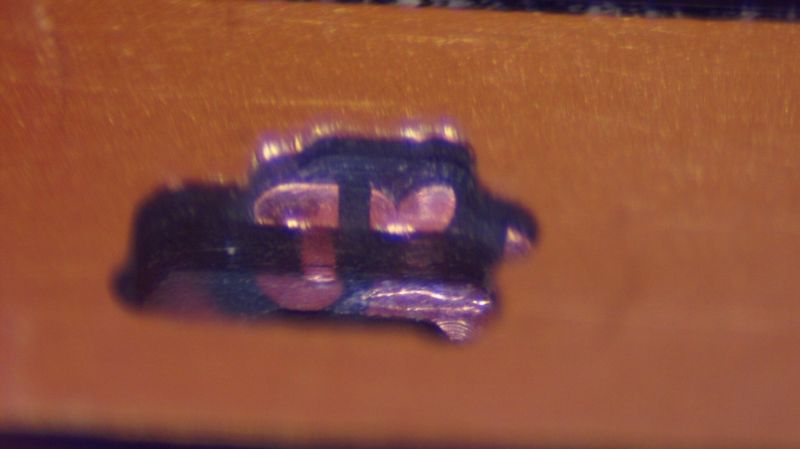
[Andrew] has only tackled one of the bodges at the time of writing, but it has to be seen to be believed. It started with milling away the PCB to get access to the blind via using a ridiculously small end mill. The cavity [Andrew] milled ended up being only about 480 μm by 600 μm and only went partially through a 0.8-mm thick board, but it was enough to resolve the internal short and add an internal bodge to fix a trace that was damaged during milling. The cavity was then filled up with epoxy resin to stabilize the repair.
This kind of debugging and repair skill just boggles the mind. It reminds us a bit of these internal chip-soldering repairs, but taken to another level entirely. We can’t wait to see what the second repair looks like, and whether the prototype for this dev board can be salvaged.
Thanks to [esclear] for the heads up on this one.


Wow! #1 having the ability to mill anything at that scale.
Wow! #2 having the ability to mill fractional depths of a PCB layer
Wow! #3 removing the PCB from the mill and returning to the same spot to mill some more at those tiny distances
Wow! #4 soldering the tiny jumper
Wow! #5 filling the tiny hole with epoxy.
I am in awe.
Yeah, everything he does is really high-end stuff. He building his own equipment because it’s all to obscene specs.
Seeing the first picture that shows the scale is a real Wow moment.
We have a product here called solder wick (generically?) I use Chemwick, it would have been good to mop up the excess solder on the USB pad. It’s like the copper braiding of a shielded cable with (or without) a bit of flux added. The one with flux is far superior.
Personally I like the one without flux – you add only what you need, to the bit of the wick in use.
https://caps0ff.blogspot.com/
It’s all about the tools. If you’ve got a FIB (focused ion beam) rework station, it makes this setup look like stone knives and bearskins. And having the tools that this guy has makes common hobbyist tools look like stone knives and bearskins. Of course, the coarser your tools, the better your skills need to be to get the job done. This is very impressive work.
I was actually just joking with someone that if these bodges get any smaller I should just take it into the lab at work and FIB it…
That’s within the territory of milling into the top of a chip package and inserting jumper wires to access data in “inaccessible” registers or glitch power supplies for a portion of a cpu.
This is actually how Apple independent repair works Today due to DRM locking hardware to stored data:
Long screw damage = multilayer board microsurgery
https://www.youtube.com/watch?v=7V7cqsBNRRE
ripped BGA pads on the CPU/NAND itself? microsurgery to dig it up
https://www.youtube.com/watch?v=M_Q7gTDSfts
blowing a short inside the CPU
https://www.youtube.com/watch?v=59-ioamwghY
https://www.youtube.com/watch?v=CoJ3eGsEBXE
There was also one where you CNCed into the CPU to remove a short, but cant find the video now :(
In that case, either of you should be well equipped to construct a mnemonic memory circuit!
Really love to know how long such a repair takes – seems like one of those repairs it actually makes no sense to bother with except as practice or for fun. Really damn good stuff though, and great production quality on the images so you can really see as a newcomer to the PCB at a glance what you are actually seeing, and what it should be.
I was actually just joking with someone that if these bodges get any smaller I should just take it into the lab at work and FIB it…
Did you follow it up with a joke that if the posts get any longer you should stop posting them on twitter? Or just stop using twitter period?
Nice work, though. I did something similar but a lot less impressive on a macbook that had the fan connector knocked off the board. Sharpened up my multimeter probes and found alternate soldering spots based on continuity readings after boring out the area beneath the connector footprint. I heard it worked flawlessly until the computer died for unrelated reasons. It’s hard work, but very satisfying.
I’m curious why Femtoduino wanted this one prototype to be bodged when they knew what the problem was, or did they not? Why not just make new boards that weren’t shorted? Surely it would be cheaper than getting you to go through all this hassle?
The goal was to verify the board before doing a respin. Six layer boards with microvias are not cheap to respin, so you want to make sure the next round is going to work.
I was wondering if he would consider FIB (focused ion beam) if the bodges get any smaller than this. But i guess I will never know.
I wonder what really went wrong with DRC there? Didn’t it properly support blind vias, or was the layer stack-up changed after the DRC was run?
I can understand the pain of “not working and nobody knows why”
A few days of micro surgery are annoying but well spent if this resolves the issue. Looks like this can be a manufacturing defect that is hard to prove even with xray.
We’ve had cases where a board house claims “sure we can do pcbs for 0.4mm BGA pitch” – and half a year later you are in a dispute why the prototype boards are not working
The defect was in the gerbers. He’s still investigating how it happened, but we’re reworking the prototype to make sure there’s no other bugs before doing a respin.
It’s fantastic work, but two things strike me as funny or odd. The first is that I just don’t get Twitter as a means to communicate things like this. It reads like stream of consciousness when people try to string tweets together, and this is one of the better ones.
The second thing though is that with all these skills, Andrew didn’t immediately think “Huh, this is a 1/32″ board” when he picked it up. That’s the first thing I notice when I pick up a circuit board. Not so much a criticism, as an observation that everyone’s different.
In the days of yore, when large multilayer PCBs rivalled the cost of the components mounted to them, repair of PCBs was an actual industry. Here’s a wonderfully 80s training video: https://www.youtube.com/watch?v=IBi40aq4-t0
That’s what I learned in the Marine Corps back in 1983. Pace was the work station supplier for the military.
This is a nearly $1K board in prototype volume with maybe $5-10 of parts on it.
Reworking the board prior to doing a new spin makes complete sense.
That’s what I was trained for in the Marine Corps back in 1983. Pace supplied the work stations for military electronics repair facilities.