PCIe, also known as PCI-Express, is a highly powerful interface. So let’s see what it takes to hack on something that powerful. PCIe is be a bit intimidating at first, however it is reasonably simple to start building PCIe stuff, and the interface is quite resilient for hobbyist-level technology. There will come a time when we want to use a PCIe chip in our designs, or perhaps, make use of the PCIe connection available on a certain Compute Module, and it’s good to make sure that we’re ready for that.
PCIe is everywhere now. Every modern computer has a bunch of PCIe devices performing crucial functions, and even iPhones use PCIe internally to connect the CPU with the flash and WiFi chips. You can get all kinds of PCIe devices: Ethernet controllers, high-throughput WiFi cards, graphics, and all the cheap NVMe drives that gladly provide you with heaps of storage when connected over PCIe. If you’re hacking on a laptop or a single-board computer and you’d like to add a PCIe device, you can get some PCIe from one of the PCIe-carrying sockets, or just tap into an existing PCIe link if there’s no socket to connect to. It’s been two decades since we’ve started getting PCIe devices – now, PCIe is on its 5.0 revision, and it’s clear that it’s here to stay.
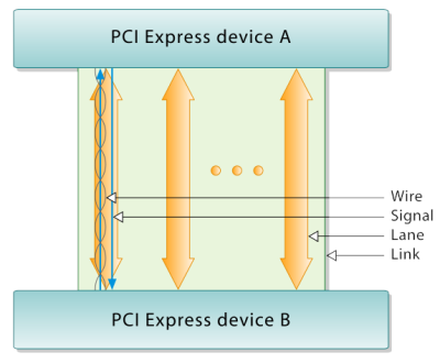
PCIe is a point-to-point bus that connects two devices together – as opposed to PCI, an older bus, that could connect a chain of devices on your mainboard. One side of a PCIe link is a device, and another is a host. For instance, in a laptop, your CPU will have multiple PCIe ports – some used to connect the GPU, some used to connect a WiFi card, some used for Ethernet, and some used for a NVMe drive.
Each PCIe link consists of at least three differential pairs – one is a 100 MHz clock, REFCLK, that is (almost) always required for a link, and two pairs that form a PCIe lane – one for transmit and another for receive. This is an x link – you can also have 2x, 4x, 8x and 16x links, with four, eight sixteen and thirty-two differential pairs respectively, plus, again, REFCLK. The wider the link, the higher its throughput!
Now, link widths in PCIe are a fun topic with plenty of cool aspects – but first, it’d be good to make sure we’re on the same page when it comes to what “differential pair” means in context of PCIe. Here on Hackaday, we’ve told you about the nitty-gritty of differential pairs before – absolutely revisit that writeup if you want to learn about differential pairs in depth! Here, I’ll quickly refresh you on the basics, and then tell you what to need to know when working with differential pairs for PCIe specifically.
What’s The Difference?
To put it simply, a differential pair is two signals, one always the opposite of another, one usually referred to as positive and another as negative. You get the logic level of the bit being transmitted by comparing the two signals against each other – instead of comparing each individual signal’s logic level to ground like we usually do, which is referred to as “single-ended”. With a differential pair, signals are close to each other and are even interwoven when it comes to cables, and as a result, any interference affects the signals equally – as signals are compared to each other to receive information, this means that the information received is not affected by noise overlaid onto both of the signals. Differential pairs also make both signals’ magnetic fields cancel each other out, resulting in the link being less noisy.
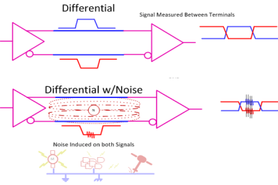
As a result, differential pairs let you crank the transmission speed up without creating noise or becoming susceptible to noise. The overwhelming majority of high-speed interfaces, as a result, use differential pairs: Ethernet, PCIe, HDMI, DisplayPort, LVDS, and even USB, although USB 2 is only pseudodifferential, USB 3 is truly differential. Resillient interfaces like RS485 and CAN use differential pairs as well. It’s easy for a hobbyist to start with differential pairs with interfaces like CAN, and USB 2 also poses no problem – at short distances, these will work no matter what, despite being differential signals and theoretically requiring special treatment.
That said, differential pairs do in fact require a bit more care when routing a PCB or putting them through cables. If you don’t take care, you risk mysterious glitches or interfaces outright not working. Let’s go through these requirements.
Treating Your Diffpairs With Respect
First off, you want to keep both of the pair’s signals close to each other throughout their length. The closer the two signals are, the better external interference cancellation works, and the less noise they radiate – given that often, multiple diffpairs run next to each other, this will help signal integrity of other pairs as well. Speaking of running separate diffpairs next to each other, you’ll want to keep them away from each other and other things – be it ground fills on the same layer, high-frequency signals. A great rule of thumb is the 5W rule, which says you need to have at least five trace width’s worth of clearance between a diffpair’s trace center and other signals. You don’t always have this much space, but it’s good to adhere to this as much as possible.
You will also want to make sure that there is an uninterrupted ground path right under these signals, alongside the entire pair – having a ground fill is ideal. Although the two signals are compared to each other by the receiver, each signal still behaves as a single-ended signal with respect to return current. Plus, a bit of extra shielding certainly doesn’t hurt. If you’re putting PCIe on a custom connector, make sure there’s at least one GND pin between each pair. Last but not least – make sure that both tracks within a pair have the same length. If your pair changes its angle, one of its two tracks becomes ever so slightly shorter, and your PCB editor diffpair tool ought to let you add a ‘wiggle’ to that track to make sure that both track lengths are equal.
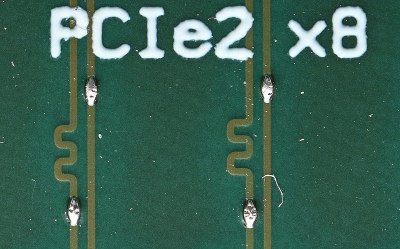
Then, there’s the little-talked-about matter – impedance matching. If you’re getting a differential pair from point A to B, you will want to make sure that you get the impedance right, and the basics of it are simpler than you might think. Impedance is like resistance, but for signals that change. Each part of the differential pair’s travel path has its own impedance: the receiver and the transmitter inside the ICs used, the IC pins, PCB traces, and any connectors or cables in between if you put the differential pair through these. At any point where impedance of the signal changes, some part of the signal is reflected from the mismatch point, and if the impedance change is significant enough, this will screw with your signal as it’s being received.
Now, this means that you have to make sure the impedance for your PCIe link is good along its entire path – which, in practice, means picking suitable connectors and tuning your PCB trace widths and spacings. PCIe hardware is mostly built with 85 Ω impedance in mind. Things like receivers, transmitters, and PCIe-intended connectors are outside your control, and to get the impedance of the entire path is reasonably uniform, you have to adjust the parts under your control to the same value. For a start, if you have to use connectors for your PCIe link, pick ones that don’t have too significant of an impedance mismatch. A good bet is using high-speed connectors or connectors built with PCIe-like signals in mind – full-size PCIe, M.2, mPCIe, USB3, USB-C, and a lot of high-speed connector families from various manufacturers.
Now to tuning the impedance of your diffpair’s PCB traces. Differential pair impedance depends on a lot of variables in reality, but if you’re a hacker starting out, there are simplified calculators that get you most of the way there – this one is my favourite. Scroll down to “Edge-Coupled Surface Microstrip”, leave track height at 35 for routing diffpairs on 1 oz copper layers, leave dielectric constant at 4.3 unless your PCB fab gives you a different value. Then, set isolation height to the distance from your diffpairs – to get that, go to your PCB manufacturer’s info and look for the PCB stackup information. Say, your diffpairs are on the top layer and the ground is on the layer right under them. For that, look for “prepreg” thickness between the top copper layer and the layer under it – that value will be your isolation height. Then, play around with track widths and spacings, aiming for 85 ohm differential impedance. The spec does give you a range from 70 to 100 ohms, even!
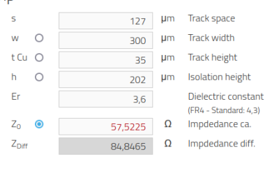 Practical exercise – let’s look at OSHPark’s 4-layer stackup. Its dielectric constant (dk) is 3.6, and our minimum trace width and spacing are both 5 mil, which is 0.127mm, or 127 μm for the calculator’s purposes; the prepreg thickness is 202 μm. Punch the dielectric constant and prepreg thicknesses into the calculator, then play with values.
You will find that increasing the track width decreases the impedance, and so does lowering the track spacing – set that one to the minimum possible. As you will see, if you choose to stick to 85 ohms, you can go for either 0.3/0.127 (width/spacing) pairs and get 84.8 ohms – way more than close enough. if you can’t afford such wide tracks, use 0.2/0.127 to get to 106 Ω – a bit outside of the recommended range, but if you must, it is alright too!
Last thing – keep your routing clean. Don’t put the differential pairs through vias to different layers if you can help it – each pair of vias adds some inductance to the signal, which can interfere with the high-speed signals. Usually, the end and start points of your PCIe link are both on the top layer – keep it this way as much as you can. If you must switch layers, add a few ground-connected vias near the diffpairs. Also, keep other high-speed and rapidly changing or noisy signals as far away from the differential pairs as you can. If you have high-power, differential-pair and single-ended connections in your projects, layout the differential pairs first.
So, five important things – route diffpairs with signals close to each other, keep ground under them, use proper connectors, adjust differential track width and spacing for the PCIe impedance, and keep your routing clean. These are the basics – it’s what you’re expected to do if you want your differential pairs to serve you well.
The Wet String Conundrum
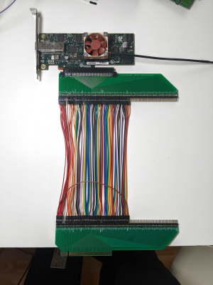 Now, if you have ever tinkered with PCIe, you might have stumbled upon some forbidden knowledge: in practice, you don’t really-really have to do all of the above.
You might have heard that PCIe runs over wet string – the first known reference to this is in a 2016 presentation on console hacking at 33C3. This is the hacker-bravado way of talking about PCIe – you can do wrong by a lot of the aforementioned guidelines when connecting PCIe devices together, and it will still chug along. And, unsurprisingly, there’s a big grain of truth – PCIe will still work in suboptimal conditions, and there’s an example after example of it in hacker and consumer worlds! Perhaps the most widely available example of PCIe abuse is passing an 1x PCIe link using USB3 cabling, something the “mining” PCIe risers do – which means that you can just go to your computer accessories store and buy a product that is only possible thanks to some PCIe abuse.
Something else that you might’ve seen and forgotten like a bad dream, is [TobleMiner] putting a x8 PCIe link through, shudder, prototyping wires – for the sake of testing out an adapter idea for cheap high-speed networking cards from HP servers, not compatible with regular PCIe slots both pinout-wise and mechanically. That prototyping setup let him design a proper version of the adapter, that we’ve later covered here on Hackaday! You can put a PCIe link through an FPC for a quick and dirty board-to-board connection, eGPU extenders have also used HDMI cables for this, and you can likely get it working with magnet wire. Here’s an experiment from Linus Tech Tips where they kept stacking PCIe extenders, and reached a five meter-long chain before the connection started becoming unstable.
PCIe is quite a bit more forgiving than quite a few other interfaces, say, USB3. There are link training mechanisms – when a PCIe connection is established, the receiver and transmitter play around with their internal parameters, adjusting them until they reach the fastest speed possible while keeping error rate low, using these parameters for the entire connection afterwards. There are also retransmissions for packets that failed to be received. PCIe has exceptional stability in practice.
It’s clear that PCIe link training has some unique parts to it – for instance, to help you make your layout better, PCIe also lets you invert any differential pair, except REFCLK, by swapping the negative and positive signals, and this will be detected and flawlessly compensated for during link training. Other technologies like USB3, HDMI, or DisplayPort don’t support such quality-of-engineer-life features. Other interfaces often require that multiple lanes should be the same length – making sure that data on one set of pairs doesn’t arrive faster than on the other. PCIe, however, is fine with across-pair mismatches as well, also detecting and compensating for these during link training. These two aren’t meant to be resilience features as much as they’re ease-of-layout features meant to help you design PCBs faster and better, but it sure helps that they’re there.
Try Your Best, No Matter What
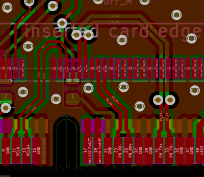
Does this resillience help hackers? Yes, absolutely – these two ease-of-layout features are used in basically any professional PCIe design, and if you’re in less sterile conditions, you can push PCIe further at your own risk. On the other hand, don’t just skirt every rule because you’ve seen someone do that – put some good-faith effort into following these five guidelines, even if you’re limited to a two-layer PCB and might never get the perfect impedance value. Following these rules will not only teach you some diffpair discipline for later projects, it will make your PCIe signals all that more resillient and error-free, and your PCIe devices more happy. It might feel good to dismiss all or some of these guidelines, since sometimes it might just work out, but the extra half hour calculating proper impedance on your board will help you ensure that your PCB doesn’t need a second revision and stays loyal to your interests throughout its entire life.
So, here’s a guideline: treat your PCIe differential pairs with respect. If you’re using a two-layer PCB and you’re doing a prototype on the cheap and you want quick turnaround time, don’t just give up on impedance because the traces would need to be way too wide to reach 85 ohms – open the calculator and see just how much you can get the impedance down anyway. Lowering isolation height lowers impedance, so consider going for 0.8mm PCB if your project’s mechanical aspects let you. Move your components around if that helps your PCIe tracks follow a better path, with less noise along the way. Perhaps link training will knock an imperfect link down a generation or two, but that’s better than not reaching a stable link at all. Put your best effort following these guidelines with what you’re given, and the differential pairs will respect your intentions in return.
For instance, if you’re using KiCad, here’s a simple demonstration on how to get a PCIe 1x link from one point to another, routing differential pairs while taking care of impedance, clearances, and via stitching.
Now, you see what it takes to route PCIe differential pairs on a board, and these guidelines will apply to all kinds of other differential pair-based interfaces. Next time, I will tell you more about PCIe signal meanings, link widths and throughput – the basics, as well as all the pleasant surprises PCIe can offer you. And, if you’re looking to go deeper into what makes PCIe tick, check out this earlier writeup of ours – it’s just the thing if making your own PCIe devices with FPGAs is what you’re looking for!

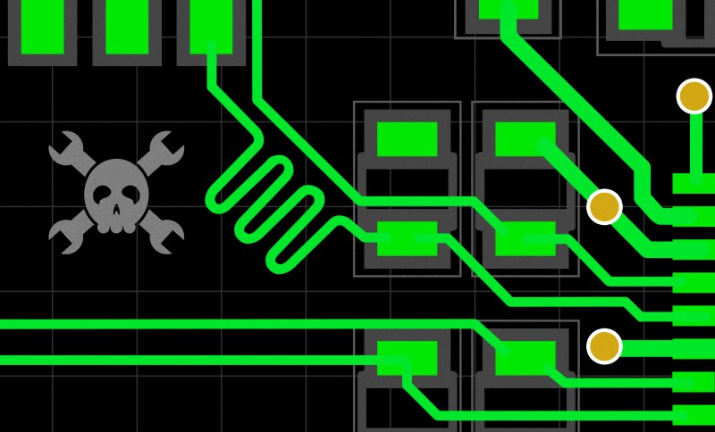


“Don’t put the differential pairs through vias to different layers if you can help it – each pair of vias adds some inductance to the signal, which can interfere with the high-speed signals. Usually, the end and start points of your PCIe link are both on the top layer – keep it this way as much as you can. If you must switch layers, add a few ground-connected vias near the diffpairs.”
One of the big issues with a 4-layer board is that the typical stackup is usually something like sig/gnd/power/sig, and so technically the bottom (or top if it’s reversed) layer doesn’t actually have a good wideband ground reference since it transitions from coupling to ground at lower frequencies to power at higher frequencies (plus also power planes tend to be more split).
So a good rule of thumb is if you *have* to change layers, keep an uninterrupted stitched ground pour on the power layer wherever the vias are. Sometimes you’ll see people suggest just putting decoupling caps near the transition, but the issue with that is that is that you’re never going to get a good flat wideband response that way. You can often get away with it, but it’s better to avoid it if you can.
It gets even more complicated with higher layer count boards, obviously, but then you can start using multiple ground plane references. But in general it’s also just good to remember that with high-speed (and low power), ground plane area’s more important than power.
Do also consider alternate stackups. Power+signal / gnd / gnd / power+signal can be a good option you don’t have to have a power plane if you can route your power.
Not suggesting this is the only one true way or anything. Just that there are alternatives that might work better for some uses.
Yup, that’s what I was trying to say in the last part. Especially for high speed/low power designs, you don’t need a ground plane.
Via’s do not have more inductance then a piece of PCB track of the same length. This is a widespread and stubborn fallacy. The problem is not inductance, but impedance mismatch between the top and bottom layer tracks.
You mention a Sig / GND / Power / Sig layer stackup, which is also not optimal, adding decoupling capacitors near the via can help, but the current path between GND and Power plane is never going to match the signal via.
A better PCB Stackup is Sig / GND (+power) / GND (+ power) / Sig.
In modern high-speed design the GND plane is extremly important, both for EMC regulation conformity, and for signal integrity. The Power does not have to be a plane at all. If it just got some solid tracks, it is plenty enough. Even a 0.12mm thin PCB track can already handle around half an amp. So to improve the layer stackup put GND planes on both the inner layers, and route some additional power on it, but not directly under high-speed signal tracks. The power tracks may even go to the signal layers. And then, when you have a layer change of your high-speed signals, also put two via’s to stitch the two GND planes together close to the signal via’s.
Yet another improvement is to remove the annular rings from the via’s in the signals, and then also approximate the gap around the via’s to match the impedance.
In this way, the impedance mismatches along the whole track are minimized. Which, uhm, leads to some other remarks about this article. The “wiggles by Phiarc” picture is also not optimal, and also creates an impedance mismatch. The wiggles should be put as close as possible to whatever causes the length mismatch. If you’ve got a 90 degree corner to the right, then put a wiggle of the size of the difference near that corner, If the mismatch is caused by a connector, then put the wiggles near that conector, etc. Imagine that the electrons going through the wires are in love and they want to hold hands. Ideally they can keep holding hands from start to finish without letting go of each other.
It’s a useful analogy, but also not great. Electrons in the wire don’t move in the same direction at the same time in a differential pair. The real reason is that it’s not the electrons, but it’s the electromagnetic field around the wire (diff pair) that contains the energy, but the result is the same. If a length mismatch is created on the left side of the PCB, and remedied on the right side (assume 10cm apart) Then those whole 10 cm are mismatched and when the energy travels along that transmission line, there is a time difference in the flanks of the signals and they tend to smear each other out.
Also, there are a bunch of great video’s about GND planes and signal integrity. As much as I’m a KiCad fanboy, altium posted an excellent (two hour long) video about GND and everything around it. Robert Feranec also has some great video’s about this and other PCB design related issues.
” The problem is not inductance, but impedance mismatch between the top and bottom layer tracks.”
For differential signals, simple vias add inductance because you can’t make ultra-tiny vias and therefore you have to spread the signals away from each other, which naturally adds inductance. You can see this easily – just “pretend” add vias, then continue routing from them on the same layer, delete the vias, and do a TDR. There’ll be an inductive jump right there.
Protip: don’t try to be fancy and provide a local REFCLK from an independent oscillator.
Always use the host’s REFCLK as it may be spread spectrum modulated for EMI compliance in most PC systems. In theory each endpoint should be able to have an independent 100MHz reference as long as it’s low drift. But an upstream clock with spread spectrum modulation is enough to make it difficult for SERDES at both ends to do clock recovery.
Ask me how I know…
If memory serves that can be turned off and on in the BIOS.
Not the case on some machines. At least Dell Precision 36xx / T76xx there’s no option. Neither do some more modern Intel NUCs.
I remember it being switchable on Athlon/64/X2/X4 boards and on Intel boards from the same era. But not since UEFI became the norm and many advanced things got hid.
being able to turn off something that is there for EMI compliance would be sketchy
The option to disable spread spectrum is there for overclocking (because it smears out the nice clean signals, so they’re less likely to be received correctly when running at unintended speeds). I don’t think I’ve ever seen a bios/efi where it wasn’t enabled by default.
I suppose disabling spread spectrum is less sketchy than having the option to (eg) pump an extra half a volt through your CPU.
You’re looking at it from a functionality standpoint. Fonz was talking about a regulatory one.
That would be true if all regulatory regimes were the same. But they’re not.
Not everything is going to have a BIOS. PCIe is used in lots of non x86 systems.
It’s virtually impossible to skip using the root’s RefClk. Some, very old and fancy mother board allowed to turn off SSC, but it’s not the case anymore and any new generation (gen3 up to gen5) will just fail with a fixed 100MHz clock.
Not strictly true across the board, since Separate Reference Clock with Independent Spread (SRIS) was developed as a solution to this, although it’s a less common feature. I think the more practical designs use a bridge or switch in the path, to provide at least one non-SSC port off of an SSC root complex. This generates a new reference clock signal and it’s possible to use the bridge/switch as a buffer to cross clock domains.
ouch =D yeah, thankfully, with PCIe, providing REFCLK is the norm!
Excellent!
“Speaking of running separate diffpairs next to each other, you’ll want to keep them away from each other and other things – be it ground fills on the same layer […]
You will also want to make sure that there is an uninterrupted ground path right under these signals, alongside the entire pair – having a ground fill is ideal.”
Uhh… ¯\_(ツ)_/¯
Huh? Ground fill on a layer below, and keep the ground fill on the same layer far away. Pretty obvious.
To make the answer as short as possible: It depends on what are the intended odd/even impedances (or diff/common mode if you like more to work with these). You make the differential impedance to match the system impedance. But the common mode impedance may (if standards allow you to) be changed according to your needs, especially if you expect a lot of interference around.
Sorry that isn’t clear!
– Add a ground fill on the layer under the pairs, and vias at each GND-connected end, like connectors in the video have.
– Don’t add ground fill on the same layer.
Take a look at a PCIe GPU – you will notice that there’s no ground fill next to the diffpairs going from the PCIe connector, and the connector’s ground pins go directly to vias.. but you can bet that there’s ground on the layer right under the diffpairs =D
This is very debatable but where I work, we generally assume that trying to do your own impedance matching is similar to trying to write assembly. We put in traces that are approximately right and then tell the board house “make these 50 ohm” (our usual requirement) and they change the dielectric thickness and trace thickness to match what their process is optimized for. As such, we always provide at least one trace width of clear space around our controlled impedance traces for them to expand the width if needed.
BTW it was really interesting and useful seeing someone else use KiCAD. I learned some new usage tricks. Watching that video was very worthwhile.
This is the way. Though it is out of reach for most of the hobbyitst, OSHPark won’t do impedance matching for you.
We work with the PCB vendors before hand to build a manufacturable and cost effective stackup which includes the trace widths. The PCB manufactures will massage the traces a little bit during production in order to increase yields. But these are usually very specialized boards with 16+ Layers and different material inlays, thermal copper coins, and much faster and delicate signals than PCIe.
Oh that seems to be the way for more pro-level fabs, yeah! For fabs like JLCPCB, OSHPark, or Aisler, it doesn’t seem like there’s such an option unless, perhaps, a hacker explicitly asks for it? Like, they give you stackup info, and guarantee some level of width/spacing precision, so that’s what, it seems, we have to work with.
Glad the KiCad video was of use! Next time, I’m defo patching screenkey to properly show keys like Esc =D
Some do. Allpcb, for instance, allows you to check impedance control and even get an impedance report.
Some of them pretend that controlled dielectric (guaranteed stackup) is the same thing as controlled impedance (guaranteed impedance) though.
“Differential pair impedance depends on a lot of variables in reality, but if you’re a hacker starting out, there are simplified calculators that get you most of the way there – this one is my favourite.”
I missed this the first time around: I *really* dislike online calculators out there. Some of them catch if you fall outside their validity limits, but not all of them.
But you still have to know what you’re doing for them: are you doing coupled stripline, asymmetric stripline, coupled microstrip, etc.? And what are those things? So if you need to know that already… why bother? There’s an actual free 2D impedance calculator out there (arbitrary transmission line calculator, or ATLC). Use that.
Coupled microstrip, for instance, can lead to *really* difficult geometries if you go with a 2-layer board, for instance. But you can just use coupled CPW-G (coplanar waveguide with ground) and figure out the ground pour spacing and it’ll be just as easy to route with a 4-layer board with close ground spacing.
Coupled CPW-G can also help to make boards vendor-neutral with higher layer boards, since the impedance will change much less depending on the dielectric thicknesses.
Most SerDes standards are designed for 4 layer or more stackup. Even USB 2.0 gets unwieldy on 2 layer standard 1.6mm FR4.
The online calculators are a pain in the ass, but short of using higher end CAD that has impedance constraints at route time, you can get by with them if you are willing to sanity check their results.
“Even USB 2.0 gets unwieldy on 2 layer standard 1.6mm FR4.”
No, it really doesn’t. That’s the advantage of a coplanar waveguide structure. Trace/space tolerances have gotten to the point where I can get 4 mil trace/space for virtually no upcharge, so the tight signal/ground spacings needed on the etch layers are not a problem anymore. And even 3 mil trace/space isn’t difficult.
The downside is that there are exactly zero good calculators out there for coupled CPW with ground, especially if ground’s far away. Hence my recommendation of ATLC.
It is really, really common for people to go to coupled microstrip calculators, plug in numbers for a 2-layer board and go “WTF, how do I do this!” Because coupled CPW-G is much less common. But it works great. The only downside (other than lack of calculators) is that process variations are larger, but it’s not anywhere near large enough to cause a serious problem.
“by swapping the negative and positive signals, and this will be detected and flawlessly compensated for during link training. Other technologies like USB3, HDMI, or DisplayPort don’t support such quality-of-engineer-life features.”
This is not accurate. USB3 standard includes polarity detection and swapping.
Hopefully the USB C series keeps going too! Was hoping to see altmode and debug accessory mode broken down as well as the other topics have been.
Though, differential pairs could be really handy or maybe essential for altmode too; if I’m reading the spec right some of the pins are at least strongly encouraged to be differential pairs (AC coupling, signals not exceeding Vtx-DIFF-PP which is a measure of differential p-p Tx voltage swing). But maybe I’m not reading it right.
Some where in the 1990’s a company i worked as a PCB designer for making network adapters and network switches and we made our own impedance test boards. These PCB’s were just over a meter long with different combinations of single and differential tracks over various ground plane combinations that we were going to use (about 5 different PCB’s in all). We would then source different signals to fly over the board to see what the true impedance was with a network analyser. The tracks being a meter long made the calculations of delay easier but they had no vias so more of a perfect world match.
If i remember correctly we found that the calculators at the time offered by online and by IPC were not very correct for impedance. We produced are own impedance calculation for use in house.
Also a lot of odd issues like finding a PCB with a solder mask and one without changes the impedance slightly. Some higher quality simulators now take this into consideration. Today i think some EM simulators are used at the higher end of the market. Also you can extract a spice model of the tracks (including vias) from some PCB design systems (mentor ICX did this) but you need a model of the driver and receiver (IBIS model).
Again there seems to be no replacement than to get a real board to know the answer of delay, impedance and mismatch.
I am missing the link to Rick Hartley presentation: https://youtu.be/QG0Apol-oj0