When all you’ve got is a hammer, everything looks like a nail. And when you’ve got a scanning electron microscope, everything must look like a sample that would be really, really interesting to see enlarged in all its 3D glory. And this is what [Zachary Tong] delivers with this up close and personal look at the chip formation process.
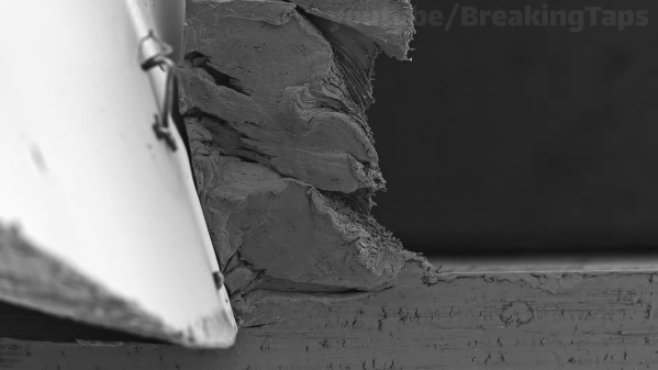
We’ve got to hand it to [Zach] with this one, because it seems like this was one of those projects that just fought back the whole time. Granted, the idea of cutting metal inside the vacuum chamber of an SEM seems like quite an undertaking right up front. To accomplish this, [Zach] needed to build a custom tool to advance a cutting edge into a piece of stock by tiny increments. His starting point was a simple off-the-shelf linear stage, which needed a lot of prep work before going into the SEM vacuum chamber. The stage’s micrometer advances a carbide insert into a small piece of aluminum 50 microns at a time, raising a tiny sliver of aluminum while it slowly plows a tiny groove into the workpiece.
Getting the multiple shots required to make a decent animation with this rig was no mean feat. [Zach]’s SEM sample chamber doesn’t have any electrical connections, so each of the 159 frames required a painstaking process of advancing the tool, pulling down a vacuum in the chamber, and taking a picture. With each frame taking at least five minutes, this was clearly a labor of love. The results are worth it, though; stitched together, the electron micrographs show the chip formation process in amazing detail. The aluminum oxide layer on the top of the workpiece is clearly visible, as are the different zones of cutting action. The grain of the metal is also clearly visible, and the “gumminess” of the chip is readily apparent too.
For as much work as this was, it seems like [Zach] had things a bit easier than [Ben Krasnow] did when he tried something similar with a much less capable SEM.
Continue reading “Getting A Close-Up View Of Chip Formation With An SEM”