Despite being much in the zeitgeist lately, we have to confess to still being a bit foggy about exactly what memristors are. The “mem” part of their name seems to be the important bit, implying a memory function, but the rest of the definition seems somewhat negotiable — enough so that you can make a memristor from a bit of photochromic dye.
Now, we’ll leave the discussion of whether [Markus Bindhammer]’s rather complex optical memory cell officially counts as a memristor to the comments below, and just go through the technical details here. The heart of this experimental device is a photochromic dye known as cis-1,2-dicyano-1,2-bis(2,4,5-
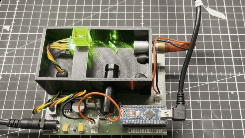
To accomplish this trick, [Markus] filled a quartz cuvette with a little CMTE-doped epoxy resin. Inside a light-tight enclosure, two lasers — one at 405 nm wavelength, the other at 532 nm — are trained on the cuvette through a dichroic mirror. On the other side of the CMTE resin, he placed a VEML7700 high-accuracy ambient light sensor. An Arduino Nano reads the light sensor and controls the lasers. Writing and erasing are accomplished by turning on the proper laser for a short amount of time; reading the state of the cell involves a carefully timed pulse from the 405 nm laser followed by a 532 nm pulse and watching the output of the sensor.
Is a one-bit memory device that uses a dye that goes for €300 per gram and a pair of laser diodes practical? Of course not, but it’s still pretty cool, and we appreciate all the effort and expense [Markus] went to with this one. Now, if you want some fuel for the “It’s not a memristor” fire, memristors might not even be a thing.


One correction: It’s not a one-bit memory. Actually you can store many states of illuminance.
Which is even cooler!
Please help me understand what your projects are. Is this an educational demonstrator for university lectures, your channel or a proof of concept that you want to optimize for capacity later on to solve a problem you are researching. It’s interesting and useful, but where will you take these? Your channel has a lot of nice subjects that seem to steer toward a goal of yours.
If you don’t mind, please do a video where you lay out your plans. I enjoy when a scientist tells people about their project logs. Glad to see you again in the comments. You teased this project a short while ago and here it is! I can only say I love it. Very costly chemical though.
Thank you, Stefan. I like to bring together different areas of science, for example electronics and chemistry or medicine. I also love combining art and technology. And I am fascinated by robotics. Perhaps the best way to express it is with a quote from Richard Feynman: “I’m an explorer, okay? I get curious about everything, and I want to investigate all kinds of stuff.” As for the memristor presented here, the long-term goal is to build an analog computer. The next steps regarding the optical memristor are mathematical representation, optimization and miniaturization.
SLC MLC TLC QLC oh no.
The whole process is wrong. Degaussing a mixture should be done with electromagnet (an old transformer soldering iron is good) not vac** pump.
Excuse me, but degaussing is a process of decreasing or eliminating a remnant magnetic field. What has this to do with my set-up? I was talking about degassing the epoxy resin via vacuum chamber which is well known practice.
See, they don’t actually care, they just wanted to show off how much they (apparently don’t) know.
I’m sure it’s you who don’t have a clue about things becuase I bet you never used a real transformer soldering iron to fix monitor whose phospors have been magnetized by careless child. Degaussing is a real procedure and I find your criticism hostile.
I bet you’ve never baked a souffle in a submarine. What’s that got to do with this discussion on degassing?
Yes, it does help to have a clue about things.
You don’t degauss the phosphors. They aren’t magnetic. You degauss the metallic structures. Like the shadow mask.
None of which is actually germane to the discussion here.
Markus, I understand that using the 405 nm laser for readout makes the optics, alignment, and signal detection easy. Could you avoid the destructive readout by using a red (low photon energy) LED to sense the optical density, without triggering the isomer change?
Hi Paul, I have already thought about it. An IR laser would probably be better than a 650 nm laser, but every additional laser complicates the optics. But of course it’s possible.
I was thinking an LED+photodetector orthogonal to the laser path to not complicate the optical path any more, but RGB dichroic prisms are pretty easy to come by now (from 3-chip projectors), so 3 lasers might be just as easy.
Orthogonal to the cone that the 405 nm laser “burns” into the 3-dimensional molecular array, I would probably not arrange the sensor, but as you say, a dichroic prism would of course be a solution for three lasers. Thanks for the input!
I’m not sure what sort of readout you’re thinking of for greater-than-one-bit operation. The chemical change is visible to the eye in the video, so surely a diffuse reddish light from a LED would be enough to allow a camera to read out the contents in a 2d plane at a time?
Well, as technology looks forward to optical computing, this may play an important role in getting there.
Putting a UV laser in an old-fashioned EPROM to make it (sort of) an EEPROM would be more practical, but
1) less fun
2) you don’t learn anything from doing it. This experiment however, is pretty fascinating.
How fast it can transfer to next readable state? I hope it spends less than 10ns.
More likely 10 ms.