
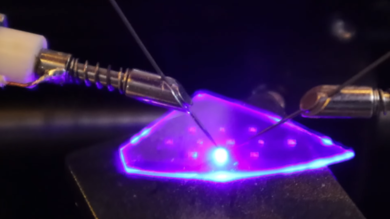
Impressive as it most certainly is when an amateur fabricates a semiconductor, most of the projects we’ve seen are more demonstrations than workable chips. [Dr. Semiconductor], however, is going much further with his fabrication process, and is already working on a method to bond chips to printed circuit boards. It’s difficult to align a PCB with the pads on the underside of an opaque silicon wafer, however, so as a trial run he’s made and bonded some transparent LED chips.
The starting material for these chips is a gallium nitride (GaN) LED epiwafer, a stacked structure of n-doped GaN, an indium gallium nitride quantum well layer, and p-doped GaN grown on a sapphire substrate. When current passes through the structure, electrons from the n-doped layer and holes from the p-type layer recombine in the quantum well layer, emitting blue light. To make a functional LED from this, [Dr. Semiconductor] needed to make electrical contacts to both the n-type and p-type layers. Making the n-type contact required cutting through the p-type and quantum well layers.
This would normally be done with reactive ion etching in chlorine, but [Dr. Semiconductor] came up with a new process: a 355-nm ultraviolet etching laser causes GaN to break down into gallium and nitrogen, with the resulting cut being cleaned up by a potassium hydroxide etch. To deposit the contacts themselves, [Dr. Semiconductor] formed a photoresist mask, deposited metal (nickel, silver, and titanium) in a sputtering chamber, and used a developer solution to dissolve the mask and lift off the unwanted metal regions.
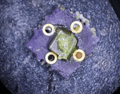
When [Dr. Semiconductor] applied current between the two contacts, the LED glowed bright blue. The next step was to mount it to a PCB; to do so, he first sliced the wafer into individual LED chips with the ultraviolet laser. He then electroplated indium bumps onto a printed circuit board, positioned the chip above these bumps, added some rosin flux, and melted the indium bumps. This soldered the chip to the board and let the board power the LED.
Like most commercial white LEDs, these were blue; most LED assemblies additionally include a phosphor layer which absorbs blue light and emits another color. To create a white LED, for example, [Dr. Semiconductor] mixed cerium-doped yttrium aluminium garnet phosphor powder with clear silicone and spread it over the LED. This absorbs some of the blue light and emits yellow light, and the resulting mixture of blue and yellow light looks white to human eyes.
We’ve previously covered some of the history of LEDs and the phosphors which make them useful. This seems to be the first inorganic LED we’ve seen, but we’ve also seen a few homemade OLEDs.
Thanks to [SpuriousIndices] for the tip!









I was quite literally thinking the other day that if we can — theoretically — make diy RAM then an LED shouldn’t be impossible either.
Glad to see that is actually the case.
I guess the next step is to dope some of that YAG and make laser diodes.
“yttrium aluminium garnet phosphor power” should be “[…] powder”
Oops. Thanks for the correction!
“Like most commercial LEDs, these were blue” – that is such an amazing thing considering the history of LEDs and the color blue. (I’m not arguing the fact, I expect it would be true with the push between blue and white LEDs pushing it far into the most produced category).
I do remember a time where leds were any color you wanted as long as it was red, amber or green… blue were barely starting and really expensive with poor eficiency…
And now they’re the brightest and most efficient, last i checked they were rapidly approaching 50% electricity to optical flux efficiency!
You can also build whatever colour you want on top of a blue LED using phosphors, for example the lime and pink COB “filaments” .
My first blue LED costs $20 in the early 90’s.
Yes, this is quite impressive to do on your own
What I hope to see with these projects is that a maker focused little silicon fab comes about.
We don’t need super tiny transistors, so we should be able to find a way to bodge something together that will still have a high success rate.
Base everything around using DNA for computing and memory.
What for?
Doesn’t require a TSMC level lab to getting anything done.
so your computer can give you a virus in real life
“maker focused little silicon fab”
A hobby-maker market is very unlikely to reach critical mass to drive the price down to a reasonable number and the chemistry is complex and expensive.
And Dr. Semiconductor is actually Matthew Hartensveld, PhD. http://www.matt.engineer/
This is cool and all but he didn’t actually make the LED material, he just bought a wafer with the n-type, p-type and quantum well already in place. (although I suspect that the stuff you would need to do the doping is well beyond the realm of a backyard hobbyist)
Yeah without taking away from the engineering feat involved in connecting to the layers this was very much a misleading title.
title should be “Packaged”
Very cool.
I like the comment that it looks white to the human eye.
We should remember that we don’t actually see violet (or a bunch of other discrete colors). Most stuff with color (paint, TVs, monitors, Kodachrome) only synthesize 3 colors’ intensity to fool the eye into thinking it’s a specific color. And that isolated violet spectrum doesn’t have any red or blue in it. Color is an optical illusion. And there’s no mixing of 2 colors to make a third. Except through very specialized nonlinear or fluorescent processes. It doesn’t happen except in the human eyeball and brain.
So… Insects may see violet and yellow combined as 2 simultaneous colors.
Starship models clear warp grill inserts need to be LEDs with tabs being connectors.
Or, you could have Mantis Shrimp eyes and are thought to see a mix of 16 base colors.
Obligatory Oatmeal reference:
https://theoatmeal.com/comics/mantis_shrimp
Unfortunately for the shrimp, the current scientific consensus is that they lack the neural structures for complex colour integration.
It’s less “mind bending palette of indescribable hues” and more “about 16 separate colours, but very fast”.
Impressive!
Mahalo
Beats using high voltage and dill pickles.