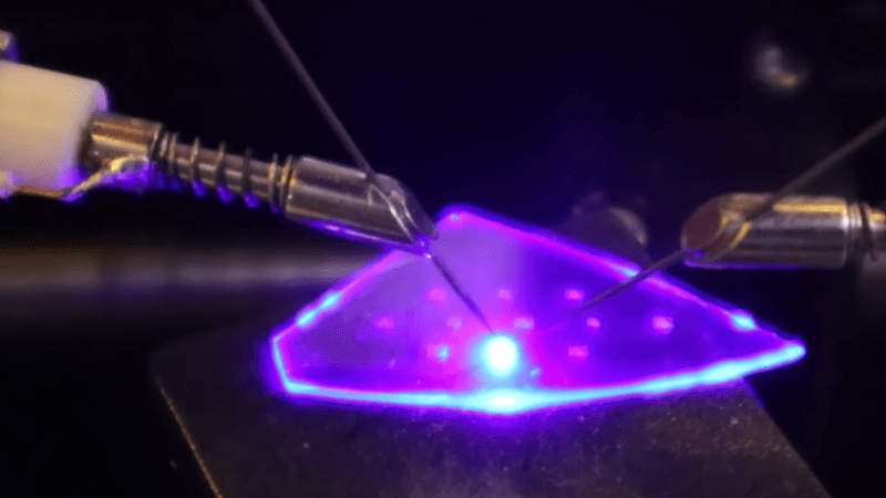
Impressive as it most certainly is when an amateur fabricates a semiconductor, most of the projects we’ve seen are more demonstrations than workable chips. [Dr. Semiconductor], however, is going much further with his fabrication process, and is already working on a method to bond chips to printed circuit boards. It’s difficult to align a PCB with the pads on the underside of an opaque silicon wafer, however, so as a trial run he’s made and bonded some transparent LED chips.
The starting material for these chips is a gallium nitride (GaN) LED epiwafer, a stacked structure of n-doped GaN, an indium gallium nitride quantum well layer, and p-doped GaN grown on a sapphire substrate. When current passes through the structure, electrons from the n-doped layer and holes from the p-type layer recombine in the quantum well layer, emitting blue light. To make a functional LED from this, [Dr. Semiconductor] needed to make electrical contacts to both the n-type and p-type layers. Making the n-type contact required cutting through the p-type and quantum well layers.
This would normally be done with reactive ion etching in chlorine, but [Dr. Semiconductor] came up with a new process: a 355-nm ultraviolet etching laser causes GaN to break down into gallium and nitrogen, with the resulting cut being cleaned up by a potassium hydroxide etch. To deposit the contacts themselves, [Dr. Semiconductor] formed a photoresist mask, deposited metal (nickel, silver, and titanium) in a sputtering chamber, and used a developer solution to dissolve the mask and lift off the unwanted metal regions.
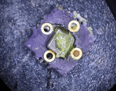
When [Dr. Semiconductor] applied current between the two contacts, the LED glowed bright blue. The next step was to mount it to a PCB; to do so, he first sliced the wafer into individual LED chips with the ultraviolet laser. He then electroplated indium bumps onto a printed circuit board, positioned the chip above these bumps, added some rosin flux, and melted the indium bumps. This soldered the chip to the board and let the board power the LED.
Like most commercial white LEDs, these were blue; most LED assemblies additionally include a phosphor layer which absorbs blue light and emits another color. To create a white LED, for example, [Dr. Semiconductor] mixed cerium-doped yttrium aluminium garnet phosphor powder with clear silicone and spread it over the LED. This absorbs some of the blue light and emits yellow light, and the resulting mixture of blue and yellow light looks white to human eyes.
We’ve previously covered some of the history of LEDs and the phosphors which make them useful. This seems to be the first inorganic LED we’ve seen, but we’ve also seen a few homemade OLEDs.
Thanks to [SpuriousIndices] for the tip!